Route to Control Vias

Planning via placement can improve the routability and integrity of the PCB.
There are many schools of thought as to the best way to route a board, but one thing that most have in common is controlling the number and the location of vias. Designing entirely without vias would be optimum but is usually not possible. However, careful placement of vias can benefit routing channels, be used to set up rows and columns, improve the signal integrity and return path and use fewer routing layers.
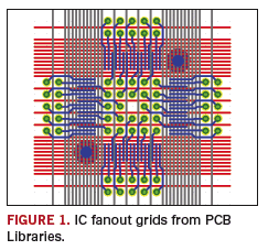
It can be very productive to use a "fan out grid" when planning routing. Fan out grids may have different priorities, but in basic form, they are the placement of escape vias from pads such that signals and their return currents can pass between via sites on any layer of the board. This is good for signal integrity because it keeps the signal and its return current closely coupled to one another. FIGURE 1 is an example of IC fan out grids from PCB Libraries.

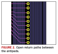
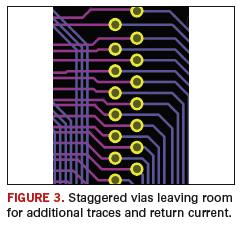
When a single routing area requires many vias, a strategy should be found that will take up the fewest routing channels. The simplest way is to line up the vias in a row, taking care to keep return paths open between the antipads of those vias, as shown in FIGURE 2. Another possibility is to stagger the vias in a slightly east-west (or north-south) arrangement so that there is room for additional traces and return current, as shown in FIGURE 3. This takes up only slightly more room than a single line of vias and provides a better chance of keeping the antipads from overlapping, thus interfering with return current.


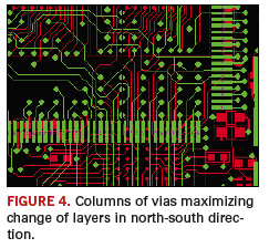
When looking at an area for routing, it is usually easy to see if there are more traces that need to be routed in an east-west direction or a north-south direction. In this case, care in planning of via placement will help to leave the most trace routing channels available in the direction they are needed. For instance, if there are many traces needed in a north-south direction and only a few in an east-west direction, one can set up columns of vias that maximize the change of layers in the north-south direction, as illustrated in FIGURE 4.

It is usually a good idea to route a bus or a group of signals on a single layer whenever possible. This allows for the best use of an area of the board and limits the return current of the signals to a single layer as well, which is good for signal integrity. When there are no vias, there is no interruption in routing channels that might be needed on other layers. It may take a little thought to do, but the benefit is felt in routing layer after layer throughout the stackup.
Designers hear about the pros and cons of autorouting boards, but it definitely takes a back seat to hand routing in the area of via placement. Even with carefully worked out constraints, an autorouter just cannot match what a designer can do with via design.
These are just a few of the ways to use via placement. If we are careful and plan for the placement of vias in the boards we design, we will definitely help the routability and integrity and the number of routing layers of the boards we design, so it is well worth the effort. PCD&F
Susy Webb is a senior PCB designer at Fairfield Industries in Houston, TX, and is a regular speaker at the PCB Shows, This email address is being protected from spambots. You need JavaScript enabled to view it..


