Simulation: The Need for Speed
Establishing selection criteria can help determine the best simulation model for a specific task.
The jitter specifications for SerDes (Serializer/Deserializer) interfaces keep getting smaller, and the timing margins for memory interfaces, like DDR3, keep shrinking until they are almost gone. As design margins shrink, PCB designers need to be able to predict how designs are going to behave in order to avoid costly re-spins and rework.
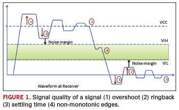
The goal of any signal integrity simulation is to validate that the interfaces on the PCB design will meet timing and noise margin specifications. By using simulations at the right times in a PCB design flow, costly board spins and rework can be avoided, as illustrated in FIGURE 1. Simulations give the designer a window into what is happening in a system. A typical process flow involves pre-layout and post-layout simulations. At the pre-layout phase, major or minor simulation work can be performed. For new designs, simulations can be used to find the best topology for an interface bus and validate IO buffer characteristics such as drive strength and edge rate. For interfaces, like DDR3 that require a detailed timing analysis to ensure that setup and hold times are met under various conditions, simulations are the only way to achieve that goal. The results of the pre-layout simulations can be used to develop layout rules so the PCB will meet specifications. These layout rules can often be used in a CAD constraint manager tool to help automate the process. For post-layout simulations, the actual board topology and routing are extracted from the CAD database to verify that the interface will work as designed. This phase can be used to validate the layout rules developed in the pre-layout phase.
New Challenges in SerDes Design
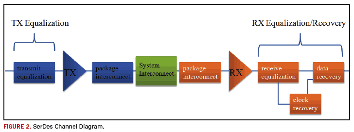
Implementing high speed SerDes devices can be complicated and time consuming– especially with new technology standards like PCI Express Generation 2.0 that have frequencies above 5 Gbps. This new wave of SerDes devices presents challenges to simulating and measuring a design. To compensate for the channel loss seen at 5 Gbps, designers are using advanced circuit techniques, like equalization and clock recovery, to open the eye back up at the receiver. Traditional SPICE (Simulation Program with Integrated Circuit Emphasis)-based models do not easily model these advanced techniques, and tools such as Matlab are often used to develop the algorithms to describe these implementations, as shown in FIGURE 2. Modeling formats such as IBIS-AMI (Input/Output Buffer Information Specification - Algorithmic Modeling Interface) have been developed to provide a universal standard to describe these algorithms so that they can be used across EDA tools. Using traditional time-domain SPICE simulations for these SerDes interfaces is no longer feasible, as the bit error rate requires simulating millions of bits. This has brought on a new wave of statistical eye diagram methods to simulate long bit error rates in a relatively short amount of time. This statistical analysis uses the channel’s impulse response to compute the eye statistics. Measuring the actual eye at the receiver provides challenges as well because the circuit equalizations often happen inside the receiver and not at the package pin where most measurements are taken. Traditional scan chain and JTAG methods, used to test PCB designs at these frequencies, no longer work. Many are moving towards embedded instrumentation which provides the ability to view the internal signals after equalization has occurred. Some silicon vendors offer proprietary solutions for embedded instrumentation, and there is movement among various organizations that set industry standards to add support.
Memory Interfaces Require Detailed Analysis
In the past, traditional parallel interfaces often have taken a back seat to the more complicated SerDes interfaces, but with the introduction of DDR2/3, things are starting to change. With future DDR4 interfaces targeting 2667 MHz frequencies, parallel interfaces soon will have some of the same issues as SerDes designs. However, parallel interfaces like DDR2/3 have their own challenges that require simulation to ensure the design will work. The major challenge with a memory interface like DDR3 is making sure the layout and routing of the interface meets the stringent setup and hold timing requirements. After taking into account the different types of skew and loss seen in a memory bus, the remaining timing margin might measure only tens of picoseconds. The only way to be able to validate a tight timing budget like this is through simulation. The fact that there are so many variables in a memory bus, such as memory controller edge rate, termination scheme at the DIMMs and PCB trace impedance, makes the need for simulation even greater. While following manufacturers’ design guidelines can help, PCB designers are finding that in order to design a robust system that can account for full system level affects, like SSN (Simultaneous Switching Noise), performing simulations is the only way to get the correct data.
Selecting The Right IO Buffer Simulation Model
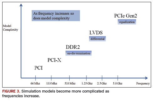
Where PCB designers were once dealing with PCI 133 MHz interfaces, they are now dealing with PCI Express Generation 2.0 interfaces with speeds up to 5 Gbps, shown in FIGURE 3. As the interface speeds have increased, so has the complexity of the simulation model representing the input/output buffer of the device. Now PCB designers have to contend with on-die termination, differential signaling and adaptive equalization in order to get designs to work.
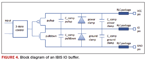
Traditionally, SPICE has been used to model the input/output buffers of a device using transistor level process data. However, by using process data, a company faces the risk of revealing the intellectual property of its design to the competition. Since there are also many different flavors of SPICE, supported by different EDA vendors, a SPICE model of an IO buffer is only good for the particular version of SPICE that can leave customers tied to a specific design tool. The IBIS specification was developed to address these concerns. An IBIS model replaces a SPICE model for use in PCB simulations in order to evaluate signal quality and timing. An IBIS model represents an IO buffer (FIGURE 4) as a behavioral model, rather than as process data. The model consists of current-voltage (I-V) data curves representing the transistors in certain modes of operation. Another side benefit of using an IBIS model is that it typically simulates much faster than a transistor-based SPICE model because it is behavioral. The IBIS specification also allows for advanced modeling, such as including external Verilog-AMS and VHDL-AMS models and an added algorithmic modeling format called IBIS-AMI for SerDes design. For advanced circuit design techniques like pre-emphasis, it requires using advanced simulation-modeling techniques that I call ‘macromodeling’. I define a macromodel as a hybrid simulation model that represents an IO buffer using a mix of modeling formats such as SPICE, IBIS and other modeling languages. For example, macromodeling would be using a traditional IBIS model with an external VHDL-AMS model to represent a SerDes IO buffer with pre-emphasis.
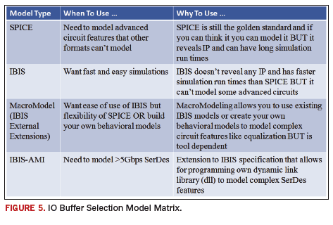
It can be confusing to determine which model format type is best for a particular simulation. To aid in this selection, one can setup a model matrix, as shown in FIGURE 5, to set the criteria for selecting IO buffer models. By using this type of selection matrix, a PCB designer can identify the best model format to use in a simulation. I typically recommend starting off with a traditional IBIS model if available. IBIS models enjoy wide support from both silicon and EDA vendors, so obtaining and being able to simulate an IBIS model is readily available. An IBIS model will also have faster simulation run times than a SPICE model. While reducing a simulation run time from three minutes to 30 seconds may not seem like a lot for one individual simulation, it can add up if you are doing hundreds or thousands of simulations. This is often the case for a memory bus configured with multiple DIMM modules that needs to have the timing verified across process and for multiple memory vendors. However, a traditional IBIS model has some limitations on modeling advanced circuit design techniques like pre-emphasis and equalization. At this point, it is a trade-off for the PCB designer to use either the traditional SPICE- based model or create a macromodel. The advantages of using the SPICE model are that design features are already there, and the model should work without any additional setup. Being tied to a specific SPICE engine and increased simulation run times are disadvantages. By selecting a macromodel, the PCB designer has the most flexibility to model the IO buffer with advanced features while limiting the simulation run time. There are some special cases, like high-speed SerDes above 5 Gbps, where a model format such as IBIS-AMI is perfectly acceptable.
Interconnect Simulation Models Need To Be Accurate
PCB designers need to be able to model and simulate different interconnect types such as packages, vias, PCB traces, connectors and cables. While an IO buffer model enjoys different modeling standards, an interconnect model can take many shapes and sizes. The more popular formats that will be discussed here are: Lossless Lumped RLC, Lossy RLGC Matrix and S-parameters. A lossless lumped RLC model is an equivalent-lumped approximation suited for an electrically short interconnect. Sometimes, these types of models are called Single-Line Models (SLMs) and Multi-Line Models (MLMs). A Multi-Line Model includes the additional coupling between elements in the interconnect. A lossy RLGC Matrix model is often derived from a field solver and is suited for uniform geometric structures like PCB traces. An S-parameter model is the scattering matrix from the RF world, suited for frequency dependent interconnects.
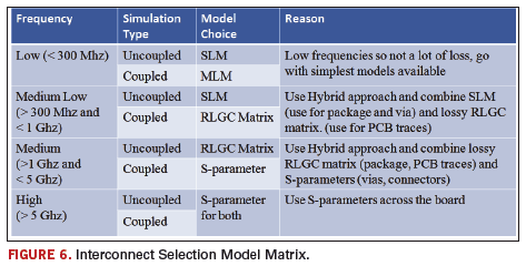
When selecting what type of interconnect model to use, there are really two key factors to consider: edge rates and loss. When edge rates reach a point fast enough so that an interconnect starts to look like a transmission line, more accurate models that include loss need to be used. As frequencies increase, so does the loss of different substrate materials in the interconnect. Model formats, like S-parameters that can model these affects, should be used. A third factor, the type of simulation to be performed, can be introduced to make the selection criteria easier as well, such as, whether a PCB designer is going to simulate crosstalk using coupled interconnect models. This can impact the selection of an interconnect model format. Again, a model matrix can be developed (FIGURE 6) to aid in the selection of an interconnect model type. In the example of an interconnect model matrix, the loss-versus-simulation type is displayed as a selection criteria. More advanced model matrices can be developed to include edge rates and other factors. When dealing with low frequencies, I recommend using simpler models because the loss is constant. Once you enter the medium-low frequency ranges, you can start to mix in lossy models in a hybrid approach to balance the trade-off between model accuracy and simulation run time. At high frequencies, I recommend going with all S-parameter models to ensure the most accurate models are used.
There are many trade-offs and equally valid methods to model and to simulate interconnects using multiple model formats. For example, you can model a PCB trace at high frequencies using a lossy RLGC Matrix generated from a field solver that includes frequency dependent effects for the conductor and dielectric loss. This type of model can be as accurate as a lab-measured S-parameter covering a wide frequency range. The idea of using selection criteria like a model matrix can help a PCB designer understand the multiple model types available and compare the benefits of the different model types against each other.
Summary
With complex interface designs like advanced SerDes, a PCB designer needs to be able to simulate and validate a design before it is taped out to make sure it will meet specification and avoid costly rework. In order to get useful simulation results, the right simulation models need to be used for the IO buffer and interconnect in an interface. By developing a selection criteria such as a model matrix, a PCB designer can easily determine the best simulation model to use and make informed design choices on how to put these models together in a simulation environment. PCD&F
Timothy Coyle is principal consultant and owner at at Signal Consulting Group LLC. He can be reached at reached at This email address is being protected from spambots. You need JavaScript enabled to view it..


