Automating the DDRx Interface Verification Process

Today's standard interfaces are more complex so that both timing and signal integrity need to be a part of the verification process.
If you’re a digital designer, there is a high likelihood that you have used Double Data Rate (DDR/DDR2/DDR3) memories in your designs — they are cheap and fast. Unfortunately, you’ve also probably discovered that verifying the razor-thin timing margins of these interfaces is very complex. With DDR2 pushing 1066 MT/s and DDR3 scheduled for 1600 MT/s, we face the demands of picosecond resolution, including “derating” adjustments to measured delay numbers based on the shape of the receiver waveforms. This is important stuff!
This kind of problem begs for a computerized solution. Don’t get me wrong, to an experienced engineer, no single measurement is too complicated; rather, with DDRx, it’s the shear number of possibilities to consider that makes complete manual verification virtually impossible. Fortunately, tools can be built to automate this tedious process and make it possible for any system designer to confidently and efficiently verify DDRx interfaces before committing to PCB prototypes.
In a recent survey of tool users, the second most important issue for engineers performing analysis was setup time and complexity. The most important issue is now — and always has been — modeling: finding or creating IBIS models. Even the effort of setting up for DDRx analysis can be eased by using a well-established and proven process of parameter-gathering user interviews, which ensure that every required step is understandable and completed. Just as important is ensuring that every non-required step is eliminated.
PCB-level timing analysis has been going through changes over the last decade. As system designers use larger building blocks connected by standard interfaces to create their products, more of the value for the system comes in the form of integration of these blocks and the software that runs on them. Timing analysis at the PCB level has become focused on verification of these standard interfaces, and the register-level circuit design is now done in RTL and implemented in an FPGA or ASIC, which becomes one of those building blocks. Timing analysis inside an IC remains much as it has in the past, where path-analysis and state-machine-sequence features are extremely important. But for PCB-level analysis, designers now need to validate very specific interfaces (like DDR memory, SATA, PCI Express, etc.) and the paths between the high-level standard blocks.
Timing requirements for these standard interfaces are spelled out in great detail, cycle-by-cycle; some are even covered in JEDEC standards. So what a designer needs are tools that are already set up for specific interfaces. The issue users have with setup for analysis is that it can and should be done by the tool vendor, not the user. So the best, most-productive timing tools for PCB-level design are interface-specific verification tools. Let’s take a look first at an example of one of these interfaces, DDR2, and get a feeling for why creating a tool as I have described would be such a productivity boost to the system designer.
What is DDRx?
DDR/DDR2/DDR3 memories have become ubiquitous in digital design exactly because they are cheap (due to the huge volumes) and fast. The speed comes from the fact that data is transferred on both the rising and falling edges of the clocking signal and from the tight margins allowed by "source synchronous" clocking. Source synchronous means that the clock and the data are sourced from the same device. Keeping the clock and the data together eliminates the manufacturing variation you would normally get using a global clock sourced from a different device than the data it’s clocking. Coming from the same device, they share any process (P), voltage (V) and temperature (T) variations. To implement this approach, data is broken up into "lanes,” where each of these lanes, or groups, has its own associated clocking strobe, again sourced from the same device. What’s the big benefit? Speed! But, at the higher data rates, timing isn’t the only problem; now signal integrity enters the picture and on-die termination (ODT) has been added to improve signal quality and to allow for those razor-thin margins. Because we are talking about bi-directionality for some signals, these terminations have to change on-the-fly, to have the proper effect for all types of read and write cycles. That, of course, means they must be taken into account during any kind of simulation. There are many issues, and it really complicates the setup for simulation.
ISI and Derating
With data rates greater than 1 GigaTransactions/second, bit periods are less than one nanosecond, which means there’s a high likelihood on most PCBs that one bit will not have arrived at the receiver before the next bit is sent on its way – an effect called “intersymbol interference” (ISI). In other words, each bit affects subsequent bits due to reflections, crosstalk and other signal integrity problems being still active as the next bit begins its journey. That, in turn, means delay values and slew rates are changing on every edge and are dependent on the specific sequence of values in the bit stream (and the sequence on neighboring nets in the byte lane). Changing delays based on the stimulus to the channel produces jitter, which must be taken into account for each timing calculation (i.e., setup and hold time). Since jitter effects vary based on the stimulus sequence, designers generally use a pseudo-random bit sequence (PRBS) of 256 bits to 1024 bits to try to stimulate something close to the worst-case jitter. It should be noted that it is possible to predict exactly the worst-case pattern and use it — a powerful methodology.
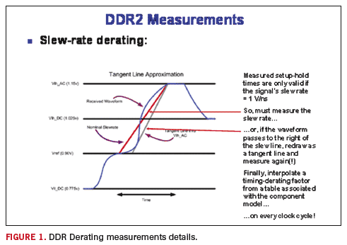
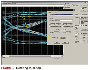
Now comes the pièce de résistance: slew-rate derating. Because DDRx margins are so tight, timing specifications have been generated based on “clean” signals with an assumed, nominal slew rate. But of course, this will never occur for all transitions on a real board (remember ISI, signal integrity and terminations, etc.), so a system was established to add or subtract from measured delay times based on the shape of the signal at the receiver. This method of measuring the slew rate (FIGURE 1) must be determined on each edge of each signal at each valid receiver, and the variance from nominal then becomes an index to find the delay-derating value in a lookup table (FIGURE 2). The lookup table is nearly always the JEDEC standard for memory-device receivers, but usually a vendor-specific table for memory controllers.


Does that seem complex? Hold on, because there any more things to worry about in trying to simulate one of these interfaces, for example:
- Each byte lane has its strobe, which must be simulated together with each data bit – with or without crosstalk
- Read Cycles from each bank, with ODT set properly
- Write Cycles to each bank, with ODT set properly
- 4 measurement threshold at receivers
- Measurements, measurements, measurements
That should make the case that setting up for proper validation of a DDRx interface is a huge task, and the actual measurements, in number and complexity, are even worse. So let’s talk about a solution.
PCB Design
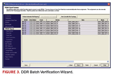
FIGURE 3 shows a step-by-step wizard. It is constructed by experts in DDRx timing and signal integrity (rather than accountants), and basically interviews you to understand everything about your particular design necessary for successful simulation. Things that affect the verification of your interface — like signal grouping, controller models, stimulus selection, memory speed, physical configurations, on-die termination behavior and derating-table selection– are all saved in a file to be used as often as needed for this interface, and possibly reused for others like it in the future. (Remember that second issue!)

But what about designers’ number one issue - getting models? Fortunately, memory vendors have traditionally been strong at creating IBIS models, both in availability and quality, probably because it made a difference in design wins! DDRx models are no different: designers can go to a memory suppliers’ sites and get IBIS models that include the necessary constructs, such as the ODT options implemented with the IBIS “model selector” keyword. Availability of the IBIS models allows tools to automatically simulate all the termination configurations that occur in the real interface.
DDRx controllers are admittedly somewhat different: sure, we can generally get a component-level IBIS model, but we also need a timing model against which to run the interface’s timing checks. These models are not readily available (yet) in a standard form, but their parameters (only a small number) are called out in various datasheets. Still, it’s important to make generating controller models a straightforward task, since our goal is productivity. So, a wizard-based interview can be used to good effect here as well. The wizard walks the user step-by-step through the required parameters (with detailed explanations of what each one means and how it’s usually seen in a data sheet), and at the end, generates the model automatically (with no need to know syntax, etc.). This is exactly what is shown in FIGURE 4: very easy model creation.
Imagine that you stepped through the interview process and filled in the answers. Then, with one more button click, the tool goes off and does a complete analysis. For a 32-bit DDR2 interface, that means over 1,500 different simulations and over 100,000 separate measurements! In the end, reports are created, starting at the top with an overall pass/fail indication, and then details on each signal, each setup and hold time and exactly where any violation occurred is detailed. The reports include actual waveform data so the designer can cross-correlate from the report to the actual signals to see precisely what happened. As mentioned early in the article, it’s all about productivity, and that’s exactly the result with a solution like this. I also mentioned in my introduction about many other standard interfaces (besides DDRx) — fortunately, there’s no reason that a similarly powerful approach couldn’t be used for those interfaces as well.
Conclusion
Times have indeed changed. PCB-level timing analysis is very different than it was a decade ago. Today you have more standard interfaces between standard building blocks. Examples are the DDR/DDR2/DDR3 interfaces for memories. These interfaces are, however, much more complex in their behavior than earlier generations, and both timing and signal integrity must be taken into account in verification of the physical implementation. Because of this complexity, measurements, both in number and difficulty, have become manually unmanageable. But it turns out that this is a perfect opportunity to use computer automation to continue to increase the system designer’s productivity. Leave the high-level thinking to the engineer and the tedium to the tools and the computer! The way forward is obvious. PCD&F
Dave Kohlmeier is product line director for Mentor’s PCB Analysis Tools, including HyperLynx, ICX and Quiet Expert. He can be contacted at This email address is being protected from spambots. You need JavaScript enabled to view it..


