The Influence of Final Finish on Lead-Free Assembly Reliability
Understanding the end use application of a PCB is critical in the selection of right solderable final finish for Pb-free applications.
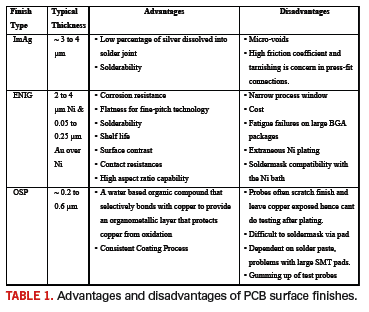
Tin-Silver-Copper (SAC) solder alloys have been introduced as primary alternatives to the eutectic tin-lead solder. The use of surface finishes is a very integral process in the assembly of printed circuit boards. The purpose of a surface finish in the manufacturing process is to provide and to maintain a solderable surface for component assembly. This is accomplished by protecting copper pads from oxidation throughout the fabrication process and up to the solder reflow process. Final finishes used in the PCB industry include Electroless Nickel/Immersion Gold (ENIG), Hot Air Solder Level (HASL), Organic Solderability Preservative (OSP), Immersion Silver (ImAg) and Immersion Tin (ImSn). It is important to understand the effects of these PCB finishes on solder joint reliability, as well as to provide an optimized process to support a particular finish. In this study, three PCB surface finishes were examined, namely ENIG, ImAg and OSP. A comparison of the above-mentioned surface finishes is shown in TABLE 1.
Test Vehicle and Assembly
All the boards were populated with CTBGA 288 packages. Each package is daisy chained to produce an overall risk-net resistance of 2 ohms. The package description is as follows: 4 rows, 0.5 mm pitch, ROHS- Compliant epoxy mold compound, die attach epoxy, die size 8.5 mm2 and a 4-layer substrate.
The component solder balls were made of Sn4.0/Ag0.5/Cu alloy and the no clean solder paste used for reflow attachment was SAC 95.5Sn/3.8Ag/0.7Cu standard paste. The solder paste constitutes around 25% to 30% of the volume of the joint after screen-printing and the reflow process. All boards were subjected to the same reflow process with a peak reflow profile slope of (Temperature vs Time) 0.5ËšC/sec. during the ascending time, a soak time of 30 to 38 sec., a peak temperature of 249.3ËšC, a cool down slope of 1.2ËšC/sec. and the time above liquidous is 35 sec.
After assembly, the boards were x-rayed for initial defects. Some defects such as bigger solder balls and solder bridging were found; however, it was not clear in this study how much they impacted the bend or drop reliability of boards. The configuration for the boards for the bend and drop tests essentially follows JESD22-B1111 with minor differences in the number of components placed, since the same board design was used for both the drop and bend test. Strain gauges were placed on bare and populated boards on both sides of the panels, and replicate readings were taken for confirmation. For cyclic bending, the validity of the constant strain assumption in a four-point-bend test has been confirmed by strain gauge measurements at all component locations across the boards. The measured microstrains from each successive run were taken at the point of maximum deflection of the PCB and compiled.2 Standard event detection techniques were used for data acquisition for both the bend and drop tests.
Bend Test Conditions
The four-point-bend test was conducted with a board populated with nine components as defined by JEDEC board level cyclic bend test method (JESD22-B111)1. An Instron Universal Tester, operating on a servo-hydraulic system, was used to conduct the bend test. Spans for the inner and outer anvils were 105 mm and 75 mm, respectively, as shown in FIGURE 1. The board was supported at the two outer anvils and loaded at two inner anvils. This provided a uniform stress region for the nine components.
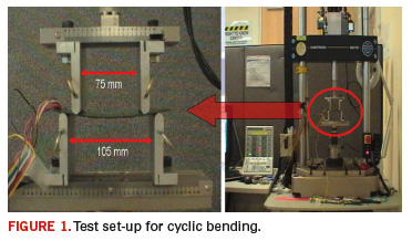
The test was performed in displacement control mode with amplitude of 1 mm, frequency of 1 Hz and 23 N preload was applied to the board in order to achieve cyclic motion. Thus, the starting position of the actuator was 1 mm below the no-load condition of the board. A sinusoidal wave was used to define the actuator cycle with the board being in either maximum deflection or no-load condition at the peak of 2 mm and valley of the cycle respectively. The board was placed such that the packages were face down and away from the actuator. Six strain gages were mounted on one board, four on the component populated and two on the unpopulated side, in order to obtain strain data at different locations.
The event detector was connected to the daisy chain circuits. Failures were recorded when the total resistance through the daisy chain network exceeded the threshold resistance of 300 ohms for 200 nanoseconds. Failure during testing was defined as the first event of intermittent discontinuity followed by an additional three such events in five subsequent cycles.
Drop Test Conditions
The drop test was conducted according to JESD22-B1111. The drop height was adjusted from 90 to 110 cm to achieve the required acceleration of 1500 G for 0.5 sec. The response was measured with the accelerometer, and the attenuation of the test board oscillations was measured as a function of time and captured using a digital oscilloscope. The boards were mounted such that the populated surface of the board was facing downwards during the test. The event detector was connected to the daisy chain circuits and failures were recorded. Failure criterion for the drop test was the same as for the bend test. When the first event of discontinuity was detected, the soldered cables were always checked to ensure that increase in resistance was not the result of any disconnected wire.
Experimental Results
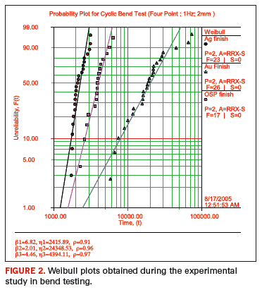
FIGURE 2 shows the Weibull plots for bend testing. It can be seen that the characteristic life for boards with ENIG finish is as much as two orders of magnitude greater than the other two types of finishes. The ImAg finish was observed to have the lowest characteristic life amongst three types of finishes. The drop test indicated several early failures that could not be analyzed to identify the nature of failures. Several failure mechanisms may have been operative. In testing, there was no clear winner in terms of characteristic life amongst the three types of finishes.
Effect of Surface Finish on Intermetallic Formations
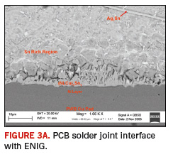
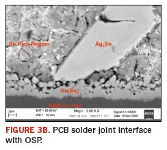
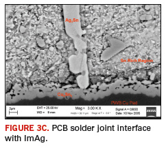
The use of different surface finishes on copper pads affects the formation of intermetallics between copper (from bond pad) and tin (from SAC solder) during the reflow process. Cu-Sn intermetallics are observed in OSP and ImAg, and Ni-Sn intermetallics are observed in ENIG finished boards. Intermetallic formations at the PCB interface, due to ENIG, OSP and ImAg, are shown in FIGURES 3a, b and c respectively. Intermetallics, being brittle formations, are generally the points of failure in reliability testing.
Failure Analysis
Failure detection was done by electrical testing. Electrical resistance of the daisy chain for each package before and after the test was compared to find the location of failures. Failure analysis consisted of visual inspection, destructive and non-destructive techniques. Components were singulated using a diamond saw and were then analyzed using optical and SEM methods. Samples were etched for 60 sec. with solution containing 92% v/v CH3OH, 5% v/v HCl and 3% v/v HNO3 etchant. Some of the packages were also tested using red dye penetration method. The packages were soaked with the dye and then baked at 100ËšC for 45 minutes. The packages were then peeled under an optical microscope. For cyclic bend, loading is due to relative displacement between packages and boards. For drop, high Gs cause large displacements and overstress trace, hence, more susceptibility of PCB failures. In the case of the bend test, the dominant failure mechanism was solder fatigue with cracks occurring in the solder joints near both the components and PCB side of the solder. Cracks were initiated at the corners and then propagated through the bulk of solder parallel to the PCB plane. In the case of the drop test, the flow stress of solder increased three to four times faster as compared to the slow plastic deformation in cyclic bend. Due to strain hardening, the tensile stress concentrated into the corner regions of the solder joints increased above the fracture strengths of the weakest reaction layers. As a result, the cracks initiated and propagated inside the interface instead of inside the bulk solder– as typically observed in constant stressed joints. In addition, the solder interconnections did not deform extensively enough under very fast mechanical loading, there was not enough driving force for the recrystallization which could generate a continuous network of grain boundaries for cracks to propagate3.
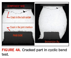
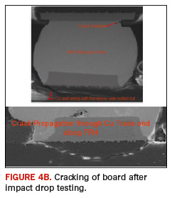
Failures occurring in the cyclic bend test for ENIG finished assemblies are shown in FIGURE 4a. In FIGURE 4b, the picture illustrates the cracking of boards that is a common observation of micro cracks in drop testing. The cracking of boards was observed in all finished boards for drop testing. In the bend test, this type of failure was typically observed in OSP and ImAg types of boards after 5000 cycles. This mechanical fatigue failure can be correlated with slow deformation failure and also with the conventional fatigue model. The localized stiffening of the PCB and the overall high strength of lead-free solder component could have contributed to the board failures. Interconnect failure under drop impact loading occurs mainly in the interface region and is determined by the properties of the intermetallic layers. In the drop test, the results that are observed in this study contradict some of the results in other studies4,5. Also, it has been well documented that Ni-Sn intermetallics are less forgiving than Cu-Sn intermetallics, which predict longer characteristic life for OSP and ImAg boards as compared to ENIG boards. Some of the reasons could be early copper trace failures or voids. Quantitatively, a high number of voids were observed for ImAg finished assemblies. ImAg has a tendency to form oxides at reflow temperature, and when organics evaporate and get trapped in molten solder, they could form the unexpected micro-voids.
Conclusion
Reliability of solder interconnections plated with three different surface finishes was examined for two different mechanical loading situations. The choice of PCB surface finishes depends on a number of factors, and it is important to consider all of them prior to product prototype build. The first consideration is the product use environment followed by reliability requirements. Some finishes may perform better in mechanical shock environments than others, while some may perform better under thermal stresses compared to mechanical shock type stresses. Also, some products may require more than one PCB surface finish: one for solderability and another for electrical contacts that experience some level of mechanical abrasion. One example of this would be the use of a selective OSP finish for solderability and a nickel-gold finish where electrical contacts are involved. Thus, a plurality of PCB surface finishes is not uncommon in modern day portable electronic products.
The interpretation of reliability data can also be complex in portable electronic products, especially when we include drop test stress testing. Solder joints, as well as PCB trace failures, can be observed. It is difficult to discern which failure occurred first since only electrical continuity is monitored and failure analysis is done at the end of the testing. Data are fitted to a statistical distribution without regard to a specific failure mechanism. PCB trace failures are dependent on the card structure and specific mechanical properties. Card thickness, number of layers in the multilayer board, trace characteristics and the nature of trace entry to the pad each have an effect. It becomes important that test vehicles closely match and mimic the product cards. Even then, differences in results, some times conflicting, cannot be ruled out.
The failure mechanisms and the reliability characteristics are dependent on the particular board and package characteristics and also on the component locations on the PCB. A comparison of reliability results from different studies can be difficult unless there is a high degree of commonality among such aspects as components, test cards, assembly processes, test parameters and failure criteria. It is important for the designer be aware of all the variables involved in the proper and judicious choice of the PCB final finishes. PCD&F
Acknowledgments
The authors thank Fahad Zahedi, Steve Dunford and Robert Darveaux from Amkor for helping to acquire the test boards, components and the facility for assembling the hardware. Authors also thank Tommi Reinikainen and Juscelino Okura at the Nokia Institute of Technology (INdT) in Manaus, Brazil, for their valuable advice and funding. This work was done at Department of Mechanical Engineering at The University of Texas at Arlington and does not neccessarily represent an endorsement by Intel Corporation.
References
1. JEDEC JESD22-B111, Board Level Drop Test Method of Components for Handheld, Electronic Products, July 2003.
2. Hossain M.M., Zahedi F., Lakhkar N.R., Viswanadham P., Dunford S.O. and Agonafer D., “ Reliability of Tin-Silver-Copper solder interconnects under mechanical loading with different PWB finishes,” Proceedings of surface mount technology international conference, 2008, Orlando FL.
3. Tee, T.Y., Ng, H.S., Lim, C.T., Pck, E., and Zhong, Z., “Board Level Drop Test and Simulation of TFBGA Packages for Telecommunication Applications,” The Proc. of the 53th IEEE/EIA Electronic Components and Technology Conference, 2003.
4. Lai Y.S., Yang P.F. and Yeh C.L, “ Experimental studies of board level reliability of chip-scale package subjected to JEDEC drop test condition,” Journal of Microelectronics reliability No. 46, pgs 645-650, 2006.
5. Zhu W.H., Xu L., Pang J.H.L, Zhang X.R., Poh E., Sun Y.F., Anthony Y.S.S., Wang C.K. and Tan H.B. “ Drop reliability study of PBGA assemblies with SAC305, SAC105 and SAC105Ni solder ball on Cu-OSP and ENIG surface finish,” Proceedings of Electronic Components and Technology Conference, Orlando FL.
Mohammad Hossain, Ph.D, quality and reliability engineer, Q&R ATD Intel Corporation; Nikhil Lakhkar, Ph.D candidate, Department of Mechanical Engineering, The University of Texas at Arlington This email address is being protected from spambots. You need JavaScript enabled to view it.; Viswanadham Puligandla, Ph.D, adjunct faculty, Department of Mechanical Engineering The University of Texas at Arlington; Dereje Agonafer, Ph.D, professor, Department of Mechanical Engineering The University of Texas at Arlington.


