A Systematic Approach to Increasing Layer Count

Increasing layer count requires an organized design approach to avoid re-spins and reduce time-to-market.
There are many issues associated with adding layers to a printed circuit board. First and foremost, the addition of layers can be the result of a customer requirement. In many case, consumer driven electronics forces designers to increase the complexity and layer count in the design.
To expedite the delivery of next generation products, designers are including more and more proven reference designs. Some of the most common reference designs include peripheral interfaces (such as USB, PCI, PCI-X, PCI-E, etc.) and memory interfaces (DDR, DDR2, etc.). These designs will typically be constructed on a pre-determined stack-up. These reference designs may also include drivers and/or receivers from programmable devices such as FPGAs. These devices are becoming a more popular choice as the central hub for two specific reasons: space reduction and proven signal integrity.
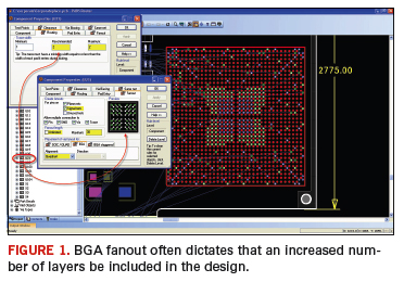
Miniaturization is another common reason why designers are pressured into adding layers to the design. Here again, consumer electronics drive the need for functional equivalents in smaller packages. This is apparent with MP3 players, cellular telephones and a host of other consumer goods. Because of this, components that incorporate greater functionality are used to replace older circuitry. These new devices are often high-pin BGA packages, which require additional layers to fan-out and to get the huge number of signals routed from the BGA package onto the PCB.
Signal integrity is also a common item of concern for this type of interconnect. The switching speeds on these devices are very fast–typically under 2 ns. Implementing designs with these types of characteristics requires exact placement and termination strategies. Smaller overall design footprints also increase the need to account for crosstalk and electromagnetic coupling between traces. Along with the increased design speeds, impedance matching has now become another important concern.
Addressing These Intertwined Challenges
The BGA fan-out. Designs that include BGA devices have the unique requirement to add additional layers to account for fan-out & escape patterns. As designers face these types of challenges, investment in adopting a PCB tool (Figure 1) that supports rules for individual decals & components is a must.
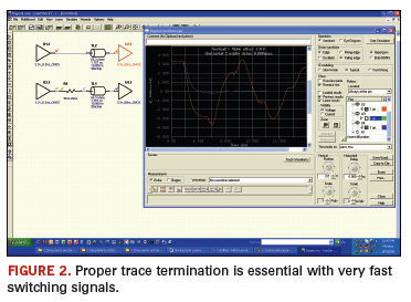
Signal integrity, switching speed & termination. As the edge rates of IC devices become faster, the requirement for understanding transmission line behavior becomes a vital part of the design process. Traditional rules of thumb that use approximations to set constraints on PCB routing lengths for traces start to fail, resulting in overshoot, ringing and other negative signal-integrity effects on traces.
Also, as these edge rates become faster, using rules of thumb can place unpractical routing constraints on traces. Take for example the rule of thumb that says traces should not be any longer in electrical length than 1/3 the rise time of the signal. Using approximately 150 ps/inch for propagation delay on FR-4 (this will vary depending on whether you’re on an inner stripline layer or an outer microstrip layer), this would mean that a bus that has signals switching with a 300 ps edge rate would need to limit the routing to less than 0.667 inches. This type of constraint will not work from a routing or manufacturing perspective and is useless.
What are the alternatives when you run into a situation like this? One option would be to place the components as close as possible to each other, while exceeding the rule of thumb, and hope it works when you get your prototype. This could be costly because it could result in many man-hours spent in the lab debugging a failing prototype and the loss of precious development time as development cycles continue to shrink.
A better alternative would be to prototype the design in a signal integrity simulation tool (Figure 2). You can perform a “what-if” prototyping here and determine if the rule of thumb you’re using is going to work. If it doesn’t, explore alternatative solutions that could improve the signal quality such as different termination strategies, IC buffer technologies or transmission line lengths. Once you find those optimal settings, you’ll have a set of constraints that you can confidently go into routing with, thus eliminating the guesswork and debug time due to signal integrity issues on your prototype in the lab.
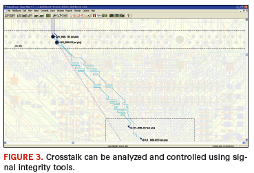
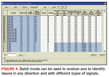
Signal integrity and crosstalk. Another side effect of miniaturization is that the traces are required to be routed in close proximity to each other, while not influencing the behavior of any other neighboring traces. To reduce errors or unexpected behavior due to crosstalk, review of the boards prior to prototype is a great benefit. Again, signal integrity tools, as shown in Figure 3, allow the designer to expose these nets either individually or via a batch process. The batch mode (Figure 4) also offers the ability to identify crosstalk in any direction, accounting for unique differences across multi-drop, bi-directional signals, which is a key differentiator for trouble-free designs.
Routing to account for impedance matching. Another key component in ensuring that traces maintain proper behavior in multi-layer boards is to account for the target impedance. A routing rule placed on a given trace that specifies a width change according to the selected layer will assist in achieving this desired behavior. By placing this type of rule on the net, the interactive routing engines will automatically adjust during the routing process.
Summary
In preparing for the leap to multi-layered boards and the new design elements contained in them, designers are reminded that software tools that include the ability to define rules and analyze multiple situations can be of great assistance. An organized design approach can avoid re-spins and reduce the product’s time-to-market. Having these tools gives the designer the power to make better decisions and to route more appropriately, while insuring the integrity of the final design result. PCD&F
John Peloso is an applications engineer for Mentor Graphics and can be reached at This email address is being protected from spambots. You need JavaScript enabled to view it..


