Design for Green: Laminates
Taking the risk for a greener planet.
The need to control hazardous materials has influenced the design of circuit boards since their conception. While the industry has worked to minimize these materials by incorporating less-toxic ones, some of these safer solutions have their own risks to the environment and the health of the population. Incorporating green laminates into PCBs is just one stage of a continuing tradition of risk management in design. In recent months, published findings regarding the safety of commonly used flame retardants has the industry rethinking previous efforts to remove all halogens from the laminate supply chain.
Recently, the European Union (EU) passed far-reaching environmental laws, known as RoHS and WEEE, that have affected the electronics industry. Japan, China, Korea and many other countries have followed suit with laws attempting to regulate products either produced or imported into their countries that may contaminate the environment. These regulations, while locally implemented, have global impacts. In a world economy, products are manufactured to the most severe standards so that there are no barriers to sales. As a result, the electronics industry has been impacted in order to accommodate these requirements.
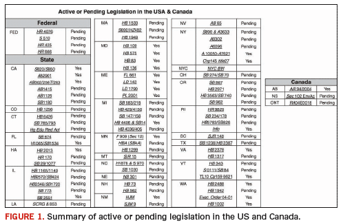
There are myriad regulations throughout North America, including those pertaining to individual states and Canada. There are additional regulations being debated by state and local governments on a regular basis. Figure 1 is a summary of many of these regulations, supplied by Dynamic Details Incorporated (DDi) of Anaheim, California. The most severe of these regulations will affect manufactured products not only in an individual state, but also in any country that the company may want to export to from its individual state.
High-Temperature and Halogen- Free Materials
Dicyanamide is a latent curing agent for epoxies commonly used before the advent of leadfree capable materials. High glass transition temperature (Tg) materials made with this curing agent have been found to have inadequate temperature capability for lead-free assembly on high-layer-count boards, although it may be adequate for some low-layer-count applications.
Multifunctional epoxies with phenolic curing agents were adopted to provide higher-temperature capabilities chemically. In addition, low coefficient of thermal expansion (CTE) inert fillers were compounded with the resins to reduce the overall change in dimension during thermal excursions. This provided higher-temperature capabilities mechanically.
For example, flame retardant materials interfere with the burning process, either by cooling or by preferentially reacting with decomposition products, excluding oxygen. As additives, their intent is to reduce the risk of injury from fire. Printed circuit boards were formulated using brominated hydrocarbons and antimony trioxide to ensure they burned slowly and were self-extinguishing. Certain sources of bromine, which includes most polybrominated diphenyl ethers and polybrominated biphenyls, have been found to have unacceptable environmental risks: they are bioaccumulative and have been banned by RoHS and other environmental laws.
Tetrabromobisphenol-A (TBBPA), the chief source of bromine in current PCB materials, reacts into the backbone of the epoxy polymer, but limits the temperature capability of laminate materials where it is incorporated. It is intended to evaporate and to decompose at temperatures that may allow flammable gaseous decomposition products to burn, and its presence interferes with combustion. This occurs above the melting point (180°C), and it is generally accepted that this occurs at a relevant rate above 230°C if unreacted. Since the lead-free assembly reflow processes can peak at 260°C or higher, the quantity incorporated into the formulation needs to be balanced with the functionality of the epoxy used.
TBBPA seems to be guilty by association with “bad” bromine containing flame retardant additives rather than by a body of evidence. The perception that bromine is bad has led to the elimination of any source of bromine in halogen-free materials. In recent months, the EU has reversed its position on TBBPA after an exhaustive eight-year-long study concluded that TBBPA does not collect in the environment and is therefore not an environmental hazard.
Halogen-free laminates have less than 900 ppm combined chlorine and bromine from any source. For the purpose of this definition, there are no restrictions on other halogens: fluorine, iodine or astatine. Fluorinated hydrocarbons, such as polytetrafluoroethylene (PTFE), are used in high-frequency applications but could be considered halogen-free in this definition. Iodine is rarely used as a flame retardant, and astatine rarely occurs in nature.
Removing the bromine requires a change in the strategy of formulating core and prepreg materials to ensure flame retardancy. A common halogen-free strategy is to incorporate materials that foam the board when it is exposed to heat and begins to melt. The foam creates a glass or char that insulates and acts as a gas barrier. Phosphate esters and melamine polyphosphates are representative of proprietary flame retardants that are compounded into the halogenfree laminates. These flame retardant additives affect thermal, electrical and physical properties of the cores and prepregs produced. NanYa NPG-170TL, Hitachi BE 67G, Taiwan Union TU-642, Nelco N4000-7EF, Isola IS500 and other suppliers have representative halogen-free materials available that exhibit some combination of acceptable material properties.
The Impact of the Design
A PCB is an electrical component with resistance, capacitance and sometimes inductance. PCBs are designed to provide electrical interconnects between active and passive devices in a minimum amount of space. Control of the board’s electrical properties is important because it affects the function of the electronic circuits.
Unfortunately, the green materials do not always have exactly the same electrical characteristics as the materials they are replacing. Altering line width and spacing, changing the distance between conductive planes or modifying the percentage of resin to glass in the cores and prepregs can accommodate some of the differences.
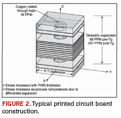
Design actions optimizing electrical properties may not result in the best performance of thermal or mechanical properties. In a typical multilayer printed-wiring board, stresses due to differential expansion during processing in a lead-free assembly are amplified by changes in thickness and layer design. Figure 2 is a detail of a standard printed circuit board construction.
Material Selection and Test
It is always desirable to define the requirements of a laminate based on reproducible laboratory tests that can be performed on different test instruments with similar and valid outcomes. For lead-free assembly of green laminates, the electronics industry has identified several test methods that, when taken together, can evaluate the characteristics and robustness of laminates. These include the following:
- The z-axis coefficient of thermal expansion (CTE) (lower is better)
- Glass transition temperature Tg (higher is better)
- Thermal decomposition temperature Td (higher is better)
- Time to delamination at 260°C, 288°C and 300°C (T260, T288, and T300) (longer is better)
- Toughness of the composite as a function of temperature
- Resistance to cathodic/anodic filamentation (CAF) growth
- Interconnect stress testing (IST)
- Highly accelerated thermal shock (HATS)
Quality and Reliability of Green Materials and Processes
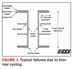
A number of accelerated fatigue and environmental tests are commonly used qualitatively to compare materials, designs and processes and to describe a material property over time. For a multilayer printed-circuit board, the integration of design, materials and value-added processes is reduced to the reliability of the z-axis connections. Failure due to thermal cycling can occur in several geometric locations, as shown in Figure 3. When a circuit board is powered and then turned off to cool, the circuit board materials — glass, resin, copper and plating finishes — do not expand and contract at the same rate. The resin in the laminate material expands at a much higher rate than the copper in the plated through hole. The copper resists the movement of the resin in the laminate and is stretched slightly during each temperature excursion. Pure copper has very little elasticity and deforms with stress, and with this deformity, the stress may be relieved mechanically through cracks that form at weak points in the metal. A typical plated through-hole construction is shown in Figure 3. During a thermal stress, caused by either turning the circuit power on or off or sequential solder during assembly, the board will expand and shrink in each direction. Failures in the conductive pathways can result in lost or diminished function of the board. These failures can be in any of these forms:
- Corner cracks
- Barrel cracks
- Foil cracks
- Post separation
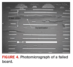
More descriptive names for failures are often required to help distinguish their causes, but these are typically subsets of the names above. Figure 4 is a photomicrograph of a failed board which illustrates the issue. The development of materials for the most severe lead-free soldering conditions requires a balance of material properties that challenge even the best laminate material formulators. The key factors include:
- The dimensional changes above and below the glass transition temperature (Tg) of the multilayer laminate needs to be less than that associated with traditional laminate materials. A reduction in the x, y and z-axis laminate changes can significantly reduce the stress placed on the plated through hole during the hightemperature solder processes.
- Adhesion to plated through-hole barrels, foils and reinforcements has to be greater at extreme temperatures to resist delamination. In multifunctional phenolic cured laminates, standard hole wall texturing and plating processes are strained, often resulting in reduced hole wall adhesion.
- Increased, void-free adhesion of prepreg to the etched core, conductors and spaces.
- Resin systems need to have higher thermal decomposition temperature Td to prevent local void formation adjacent to the plated through hole.
- Resin systems need to be able to withstand higher temperatures longer.
- Resin systems need to be robust in the presence of moisture, either by not absorbing or not being affected by it.
- New materials need to continue to meet flame retardant requirements to UL 94V0.
- New materials cannot cause significant changes in the material and processing costs of the raw laminate and prepreg.
Lead-free Assembly Impact on PCB Fabrication
Customer requirements come to board fabricators in the usual formal and informal manners: by drawings, by inside data and specifications and in the boilerplate on purchase orders. Although fabricators build to print, there is a concern when the material set or design is not consistent with the assembly process, so additional care needs to be taken to make sure that the boards will survive after leaving the PCB fabricator.
Current lead-free solder formulations that meet the RoHS directives require higher temperatures to ensure reliable joints that are equivalent legacy tin-lead solder. The existing FR-4 material sets did not behave well in all designs, so the fabricators have had to conduct extensive testing to evaluate the impact of the change in the assembly process.
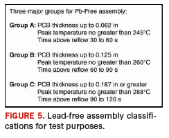
In the case of DDi, testing protocol divided lead-free assembly applications into three groups, A, B and C, depending on reflow profile and board thickness, as shown in Figure 5. The tests included thermal stability, peel strength, solder float, electrical conductivity and the IST, HATS and CAF tests. In addition, they evaluated 10 different FR-4 materials and made several classifications of FR-4 boards by material properties, as shown in Figure 6.
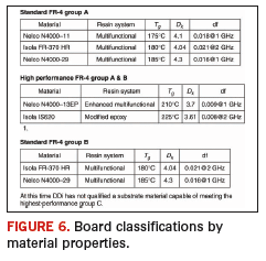
These properties include:
- Resin system
- Tg (glass transition temperature inflection point where the CTE changes due to increased molecular mobility)
- Dk (dielectric constant), the relative ability of the insulator to hold a capacitive charge as compared to free space
- df (dissipation factor), the decimal ratio of the irrecoverable to the recoverable electrical energy introduced into the insulating material when exposed to electromagnetic field
Within the industry, the IPC has published Standard IPC-4101B with slash sheets to represent generic products which can meet lead-free assembly requirements. Specifically, /126 and /129 represent materials which meet the most rigorous requirements. The specifications address tests and methods, reproducible from one lab to the next, that provide a decision point on the product produced as a raw material for fabricating boards. Board fabricators see this as an entitlement (minimum of expected properties) but are more concerned with the integration of these materials, the design and value-added processes to provide a functional board.
Summary
The EU directives and other such global regulation are driving the evolution of green laminates and manufacturing processes. Solving environmental issues requires diligence in ensuring that downstream processes are not compromised. Restricting the use of lead in PCB fabrication and assembly has required significant efforts both by material suppliers to reformulate basic products and by fabricators to tighten their processes to facilitate the use of these new materials. At this time, industry confidence and long-term reliability data on lead-free electronics does not match the substantial history that exists for traditional tin-lead products and processes. It will take more time, additional testing and substantial data collection to develop the real-time reliability information needed to assess the impact these changes have had on long-term product reliability. PCD&F
Michael J. Taylor works in research and development for Dynamic Details Inc. (DDi) and can be reached at mtaylor@ddiglobal. com. Ed note: This article has been adapted from the book “Green Electronics Design And Manufacturing: Implementing Lead- Free and RoHS-Compliant Global Products,” by Sammy G. Shina (McGraw-Hill; 2008).


