Environmentally Friendly Digital Inkjet Solder Mask
The advantages of inkjet processing provide the PCB fabricator with a new tool to improve product quality and reduce waste.
Untitled PageEnvironmentally Friendly Digital Inkjet Solder Mask
Yehuda David and Dr. Yifat Bareket
The advantages of inkjet processing provide the PCB fabricator with a new tool to improve product quality and reduce waste.
The traditional solder mask process requires expensive capital equipment and a major amount of production floor space, in both the wet process area as well as in the clean-room environment of the “yellow room.” Because of the number of steps, traditional liquid photoimageable solder mask processes involve a high number of skilled employees. The total process involves the use of a number of chemicals (developer) and the manufacture and maintenance of photo tools used to image the solder mask. While today’s solder mask materials are fine tuned, quite often the results demonstrate limited performance, long cycle time and a major contributor to the total “cost of goods” in the profit and loss statement of many PCB companies. The expected benefits from digital inkjet solder mask printing as shown by comparative tests with other systems are numerous and significant, and may include:
- flexibility with balancing line throughput
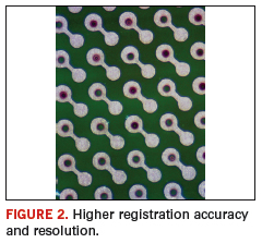
- higher registration accuracy and resolution
- ability of printing robust solder dams between fine pads
- no solder mask residue inside holes
- adjustable, selective coating thickness for conductors, laminate and power areas
- labor, photo tools cost savings, reduced cycle time and material savings
- reduced chemical waste and waste treatment costs
Inkjet digital printing allows significant simplification in the solder mask process. The one-step process also has the potential to increase final yield in both PCB fabrication and assembly. Handling (and handling related) defects are minimized in the PCB fabrication process, and “selective additive printing” technologies minimize shorts and improve yield in the assembly process.
Zero Clearance Technology
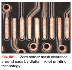
Using a traditional solder mask process with a medium pitch density SMT component, most PCB manufacturers are able to produce solder dams (used to prevent shorting during the reflow operation) with sufficient clearance between adjacent pads. However, in the case of a high-density SMT component, many PCB manufacturers cannot produce the required solder dams. One limiting factor is that there is insufficient registration accuracy between the film and the PCB in the traditional solder mask process. Additionally, with many processes there is a resulting solder mask undercut after exposure and development, which reduces adhesion of the mask so that solder dams cannot stand up to further processing. In these cases, where a solder dam is needed for advanced high-pitch components, the industry is often forced to do without, simply because the traditional processes are not robust enough to generate reliable 3 mil or thinner solder mask dams.
These problems associated with traditional processes can be avoided by digital inkjet printing, with each panel going through an individualized registration process between the CAM data and the panel prior to printing, facilitating accurate solder mask deposition, as seen in Figure 1 and Figure 2.


A Selective Printing Method
Holes. With a traditional process, the solder mask stage is applied as a non-selective coating. Typically, a double-sided screen coater or spray coater applies the solder mask material to cover the entire panel. During this process, not only are the board surfaces coated with solder mask, but the holes are partially or completely filled with solder mask as well. Removing the solder mask from high aspect ratio via holes and blind vias can be a difficult and sometimes impossible task. These non-cured residues can create numerous problems, which become especially evident during the component assembly process.
Digital inkjet printing, on the other hand, is a selective process that does not fill or coat holes or assembly attachment areas with solder mask at any time, so there is never a chance of residue.
Traces and Shoulders. Some experts believe that surface finishing anomalies, such as the “black pad” can be attributed to residue on the copper surfaces from incomplete solder mask development. In the traditional process, conductors are not always symmetrically covered, and the resulting “thin knee” areas can break down, allowing solder to bridge across traces resulting in shorts after the assembly process.
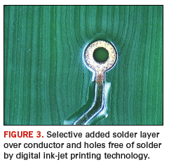
Digital inkjet printing, on the other hand, is a selective process the desired thickness of solder mask is selectively applied to the board with a proprietary coating technology that results in a symmetrical coverage of conductors, even traces that result from high copper thicknesses, using less material than the traditional methods, with a corresponding savings in material cost. (Figure 3)

Solder Mask Formulation Challenges
The solder mask has a number of functional requirements after application to the PCB. Chemical formulation is key to the cured solder mask material final properties. According to IPC-T-50, this layer is considered “a heat resistant coating material applied to selected areas to prevent the deposition of solder upon those areas during subsequent soldering.” The chemical, physical and electrical properties of this micron-scale coating are carefully detected and the final material quality should meet the IPC-SM-840D standard.
The common UV cured solder mask formulations are always a mixture of various ingredients, composed by several chemical groups, each of them added for specific purpose. The primary ingredients are as follows:
Resins. A combination of monomers, oligomers and polymers with varying chemical structure and performance, responsible for determining viscosity, basic rheology, adhesion and the dried film chemical and mechanical properties.
Fillers. A combination of inorganic particles, various surface treatment performance enhancing ingredients, and organic particles used primarily for ink stability, opacity, color, and the mechanical and electrical properties of the dried film.
Surface-active elements. A combination of surfactants including charge properties as well as basic hydrophobic and hydrophilic moieties for ink stability properties via particles stabilization.
Additives. Special ingredients such as an antifoaming agent, leveling agent, flame retardant, biocide, etc., are incorporated for both wet ink performance as well as the dried film properties.
Each one of the conventional application methods such as screen printing, spray or curtain coating requires different solder mask viscosity i.e. from liquid to past form. In addition, the particle size of the fillers in these formulations often have little effect on the overall performance of the coating.
The digital inkjet solder mask printing technology needed to reevaluate the standard solder mask parameters. All the traditional criteria were taken into consideration in the formulation of a new type of solder mask that was tailor made for both the application specifics of inkjet deposition and one that embodied both UV and thermal curing ink properties to facilitate productivity. The demands from inkjet solder mask ink properties are much more complicated than those described above for a traditional solder mask material. The task of optimizing the deposition characteristics and retaining the excellent film properties was paramount. The major differences between the approaches are as follows:
Inkjet solder mask ink viscosity. For inkjet technology, the ink viscosity is a major factor. The ink delivery system starts from a main container, continues to a middle container and ends at the print head system. In order to obtain continuous ink flow without blocking a passageway, it is essential to keep the ink at a remarkably low viscosity, usually 10-20 cps at the jetting temperature. This unusually low solder mask ink viscosity is achieved by the careful selection of resins. Maintaining viscosity, while keeping the other properties, such as curing efficiency, exactly the same, was a challenging task. The new formulation performs to the required industry standards, as well as having other essential production favorable characteristics compatible with the inkjet process.
Ink particle size and distribution. For inkjet inks, the filler particle size is critical for print head performance and maintenance. Solder mask ink must exhibit an average particle size in the sub-micron range, with a very narrow particle size distribution. This property is common for inkjet inks but is definitely unique for inks used in solder mask material.
In order to achieve this feature while keeping other essential properties, suitable raw materials must be selected as well as applying an effective grinding procedure. Minimizing ink particle size requires the addition of unique surfactants to ensure consistent ink performance. It should also be emphasized that both previously mentioned parameters are theoretically contradictory to each other, since particle size reduction tends to increase the mean viscosity.
As a result, the inkjet solder mask is a sophisticated formula that contains a high solids content with nano to micron scale particles, while maintaining very low viscosity suitable to the jetting parameters, with desirable dried film properties comparable to other industry accepted solder mask materials.
Another important factor for solder mask performance is its curing system. The inkjet solder mask ink uses two curing systems, a UV and a thermal initiated cure. This hybrid, patent pending formula integrates the benefits of each system, precisely adjusting the performance to meet the demands of the digital inkjet environment.
Considering the environmental benefits of the digital printing solder mask process, both machine and compatible ink offer an ecologically friendly approach to the development and production process. The ink ingredients were carefully selected to minimize VOC and other irritating or harmful components. The formulation is RoHS approved and the dry film passes UL 94 V-0 grade.
The PCB industry is moving aggressively into the age of digital printing, with the adaptation of inkjet printing for imaging, solder mask and legend inks. In some applications, inkjet will also be used to selectively build circuit traces with an additive application of conductive materials. The operational benefits of these systems are clear. The technological advantages that can be achieved by digital solder mask printing will have a major impact on the future of the PCB industry. PCD&F
Yehuda David is the product manager of Greenjet and Dr. Yifat Bareket is vice president – chemistry for Printar Ltd. They can be reached at This email address is being protected from spambots. You need JavaScript enabled to view it. and This email address is being protected from spambots. You need JavaScript enabled to view it. respectively.


