AOI - Defining Reliability for Complex Designs
Published: 05 June 2008
by Zulki Khan

Advanced AOI techniques provide manufacturers and OEM customers with exceptional inspection reliability.
Automated optical inspection (AOI) technology is making significant progress as PCB designs continue to pack in more circuitry per square inch and create new inspection challenges. Nowhere is this felt more than in assembly. Both designers and EMS providers need to stay abreast of the latest advances in AOI tooling to ensure that designs can be inspected to yield highly reliable assembled products. Precise optics, advanced AOI algorithms, powerful computing, and easy-to-read graphical user interfaces (GUIs) are critical to the success of PCB inspection whether it is at the bare board level or in pre- post-assembly.The common goal among AOI system manufacturers is to improve lighting, computing power, vision software, and signal-to-noise ratio (SNR). These improvements make AOI products more intelligent, flexible, and with far more repeatable results that are superior to human visual inspection. In AOI terms, SNR refers to the signal or image represented by a featured component and its markings of interest. Noise comes in a variety of forms that need to be suppressed to achieve a cleaner image.
Lighting is a critical factor for managing SNR. In the case of post-assembly inspection, the AOI tool must have the capability to view all the features and markings of a component to efficiently perform an inspection. Appropriate light conditions amplify the features of interest and verify them, while suppressing any features considered noise. LED-based lighting, now standard for newer AOI gear, is stable and easily controlled. Older style incandescent and fluorescent lighting are still used in some newer systems.
Further, the increasing complexity of PCB manufacturing is severely challenging AOI’s computing power. Hence, increasingly powerful data crunching capability is critical to acquiring an image, comparing it to a golden board, processing the inspection, and communicating the information to the database. One of the biggest challenges is that all this computing needs to happen continuously and in real time.
High-end AOI systems operate on 3-dimensional CAD data. They render an image in 3D to perform component verification for cracks or flaws, lead contamination or oxidization, scratches, and other defects. These advanced AOI systems use 4 to 6 cameras to capture an image the cameras translate the light pattern from the inspected component into an electronic image.
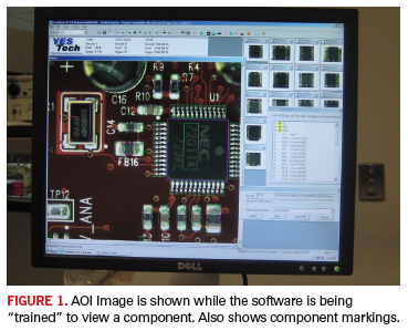
FIGURE 1 shows an AOI image while the software is being “trained” to view a component and verify markings. In this process, the system uses progressive scanning to acquire a series of images and then compares them against each other. In this training sequence, the computer analyzes the image of the board’s features to exact specifications. Here, the “brains” of the AOI system is the vision computer and its software, where complex algorithms store details and verify board images while performing the initial inspection. The results of the initial inspection are an acceptance or rejection of the stored parameters of the acquired data.

An image from a golden board is then used as a reference to compare it with images of inspected boards. Cameras scan the device under test (DUT) for catastrophic failures or missing components and quality defects, also known as manufacturing processes defects. These defects include fillet size, the shape of solder joints, and component skew, among others. The design of AOI cameras plays an important role in boosting their effectiveness. The objective here is to place the camera at an angle so that it can achieve maximum light collection for component inspection. This allows the camera to capture as much area as possible to apply a wider field of coverage to an inspected device.
AOI can be applied at various stages of the manufacturing process, including bare board inspection, and can be used to verify the inner layer stack up, lamination tolerances, and registration of layers at the bare board manufacturing level. At the PCB assembly level, AOI can perform solder joint inspection at pre- and post-reflow stages. At pre-reflow, AOI inspects for the placement accuracy of the components that the pick-and-place machine has dispensed. At post-reflow, it can check for accurate component placement after the board is processed through a reflow oven.
In the bare board application, AOI can be used to verify trace and space width and violations, as well as inspect for excessive or insufficient copper removal during or after the etching process. AOI also can inspect for trace shorts, cuts, jumps, and other defects in the manufacturing process.
Therefore, it is important for the PCB fabricator and EMS provider to use AOI inspection at various stages of the process. AOI can also serve as a process validation indicator and reduce the amount of rework and touch up at the end of the assembly process, increasing the process yield in a PCB fabrication operation.
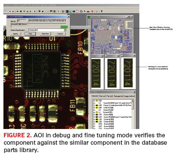
Specifically, at board assembly, AOI checks for such problems as area defects, component offsets, component polarity, component presence or absence, component skew from surface mount pads, excessive solder joints, flipped components, insufficient solder joints and paste around leads, tombstoning, solder bridges, and solder paste registration. In FIGURE 2, AOI debugs and fine-tunes component verification by comparing it to a similar component in the database parts library.

Other Key Features
Foremost among AOI features is the offline programming option, which allows a user to program the AOI system offline and avoids downtime, helping to keep the system continuously inspecting boards. This feature is both cost effective and saves time. Another important AOI feature is solder bump (blob) analysis shown in TABLE 1. This analysis verifies the presence or absence of solder on component leads.
Optical character recognition (OCR) is another useful AOI feature. More advanced AOI systems use optical character verification (OCV). Both perform character matching, status checks, and data basing, where OCR and OCV correlate text in the captured image with an image algorithm saved in the database. Based on this comparison, OCR and OCV will flag a particular image if there are flaws in the component.
AOI is especially valuable for visually defining component manufacturers’ markings. Many manufacturers can make the same component, but their markings will always be different. Therefore, it’s vital for the AOI software to be sufficiently advanced to correctly associate specific markings with the correct component manufacturer.
Staging and Lighting
Most AOI systems have built-in “intelligent” staging and lighting, which saves time in inspection and component verification. Using these options sometimes requires the installation of macro programs to utilize these AOI system features.Intelligent AOI can utilize multiple forms of lighting. One source reflects light and causes the highlighting of a particular feature, while other light sources can be used to obscure undesirable component features, which are considered noise. Hence, intelligent AOI determines the required lighting parameters, either ambient or created light, and can determine angles and the correct lighting intensity applied to a given component.
Proper staging and lighting setup reduce variability in component images. They act to properly present the image for the vision computer. Without proper presentation, the vision inspection process can be slowed, preventing AOI from properly inspecting the desired components within given time constraints.
New AOI Requirements
Today’s AOI systems are being challenged by rapidly advancing technologies that create more complex PCBs than ever before. It may become evident to a manufacturer that the AOI system being used is outdated when it can no longer detect newer and smaller packages or the minute component markings on them. In these instances, extremely high-powered camera magnification and specific angles may be necessary to accurately inspect these small packages and their markings.Accurate color detection should also be incorporated in newer AOI models. Some through-hole components are color coded like resistors and capacitors. AOI detects the colors on the bands of these devices, but often, close colors in inspection images appear similar to an AOI system, making inspection difficult. This is a problem that requires attention in future AOI development. Recognizing odd-shaped PCBs and non-symmetrical components is another improvement that can make AOI systems operate more efficiently. Due to these unusual attributes, some AOI models have difficulty inspecting these types of PCBs and components.
As for its limitations, an AOI system can be more useful by giving it the capability to import data from commonly available software applications and platforms, and be able to manipulate that data to obtain desired results. Some AOI systems have size and weight limits for the PCB. For many tools, an 18-inch by 20-inch, three to five pound board is the largest that can be inspected pre/post assembly.
The ability to produce statistical process control (SPC) data is one particular feature that would make AOI more useful. SPC comes in handy when there are recurring failures of specific components, and this feature would allow tracking by lot and date code.
On the plus side, newer AOI systems have the capability to assign a barcode to all boards passing their inspection. Plus, newer systems incorporate lights that can automatically adjust intensity for the board under inspection, increasing detection sensitivity and accuracy of the system. But what’s missing and should be incorporated into future developments is a “grey test.” This feature measures the brightness level on the tip of an SMT pad to detect a defective condition, such as an incorrect amount of solder. This problem area could be improved by the use of different and perhaps better illumination sources.
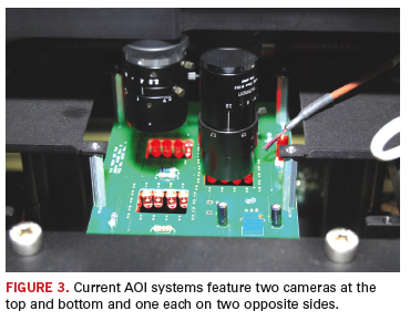
Finally, a good AOI machine has at least six cameras to inspect the top, bottom, right, left, front and back areas of a board, as shown in FIGURE 3. The quality of cameras has come a long way from those in the past, and are more powerful with considerably higher image capturing and processing capabilities. These advances account for one of the more important aspects in the accuracy of today’s AOI machines.

An advanced feature is the capability of AOI machine to be able to check and detect shorts, especially those hidden under an IC. Inspecting and catching a simple open circuit using an AOI inspection is relatively an easy task, but an improvement in existing AOI machines would be the ability to find the hard to find opens, which may require more powerful algorithms and techniques.
The alternative to AOI is human visual inspection, which is not acceptable in light of the growing complexity and reduced component sizes used on PCBs. For effective human PCB inspection, technicians typically must have 10 to 15 years experience visually inspecting PCBs, but regardless of experience, while progressing through the workday, an inspector will become tired and less efficient. As this occurs, carelessness can lead to an increasing number of board defects. That’s why advanced AOI is a “must” to provide OEM customers with the ultimate reliability in the inspection of their highly complex PCBs. PCD&F
Zulki Khan is president and founder of Nexlogic Technologies and can be reached at This email address is being protected from spambots. You need JavaScript enabled to view it..


