Improving Design Communication Using DfA Analysis and Feedback
Published: 05 June 2008
by Mark Laing

Creating a single data format from design through manufacturing can accelerate design data transfer, improving yields and reducing cost.
There are many facets that must align successfully in order to bring printed circuit boards (PCBs) from design into manufacturing operation. The ability to create an electronic design, analyze it for design and manufacturing issues, cost effectively manufacture it, and efficiently get it into a customer’s hands are keys to being successful in the marketplace. A common need across each of these different activities is the ability to understand, work and collaborate with the data that defines the product.The ability to support each of these “product realization” activities with common data and tools provides several benefits. At the heart of the matter is managing the product data to support Design for Assembly (DfA), Design for Test (DfT) and transitioning design data to manufacturing. Having a common data set to work from allows earlier and more efficient communication between the groups responsible for bringing a product to market. Ease of communication between these different groups is essential when you realize the cost of correcting manufacturing issues increases substantially as you move further from design into volume manufacturing. The cost to correct a defect increases by a factor of 10 for each step in the manufacturing process. In other words, to correct an issue at the design stage is more than a thousand times cheaper than when that product has been delivered to the customer.
Ensuring that the end product meets established quality and cost targets requires a set of solutions that supports analysis and collaboration from design through manufacturing. The process continues to build upon the underlying product information and allows manufacturers to balance the requirements of each group in the product realization chain. Being able to further define the different phases of design-to-manufacturing allows for earlier and quicker feedback from the different groups that need to participate in the review process. For example, an initial DfA analysis can be performed once the components have been placed in the layout, but before the routing phase has been started. To facilitate this, the neutral design data must be able to support partial design data. Feedback provided at this stage of the design can be incorporated more quickly than if the analysis was done after the complex routing had been completed. Often, any layout changes at this point, even seemingly small ones, can have a huge effect on the vias and traces that have already been placed.
Once the PCB layout has been solidified, the same data set can then be used for assembly documentation, optimization and programming of the production equipment used to build the product. It will also be used to create a complete test and inspection strategy that will ensure that the quality levels required are attained. Since the programs for all machines have been created from the same data set, material management and control can cost- effectively determine just-in-time parts replacement to maximize machine utilization. This level of data management is the underlying basis to support lean manufacturing, which will be the differentiating characteristic of profitable manufacturers in the future.
Complete Design Definition Data
Facilitating analysis and collaboration across the project requires a common data format to communicate schematic, layout, board, panel, bill of material (BOM), and analysis and collaboration information in a concise format. The format can be structured such that it can represent all the current design data, as well as, being flexible enough to be updated as new technologies develop. Utilizing the common data format for communication between the design and manufacturing teams allows creating the authored data from the design tool, passing that data to external teams for analysis and review and then communicating these results back to the authoring tool for possible revision. Clear, unambiguous communication of design intent coupled with analysis of manufacturing capabilities ensures product designs will benefit from shortened time to market and improved product quality.Design for Assembly
Most design teams use some method to perform design reviews at various stages of the design process; these methods may be manual, automatic, or a combination of the two. Design for Manufacture (DfM), DfA and DfT cover the primary areas of this analysis, though this is by no means a complete list of the possible types of review. The neutral data format employed across the various analysis steps provides a common platform for all results to be collected and reported. This common neutral data format also ensures that all reviewers are analyzing the same product design data, which leads to a consistent analysis of the data across the various reviewers. Typically, specific groups will be responsible for performing the different types of analysis listed above, as they are considered the domain experts in these areas. However, the results of their individual analysis need to be aggregated and shared across the enterprise to derive a complete set of results that is fed back to the design team for consideration. A further benefit of a common data format is easy adoption of low cost, easy to use viewing tools. Easy access to the information under review increases the number of groups and people who can participate in the review process, yielding better results sooner.During the review process, reviewers check the design to ensure it conforms to the design guidelines. In an automated environment these guidelines translate into Design Rule Checks (DRCs). During the analysis process, if a design rule violates the guidelines, the violation is indicated in the data with a DRC marker. DRC markers form an intelligent way to indicate a violation of a design rule; they can be used to highlight issues in the layout that need to be addressed or changed in the design prior to beginning manufacture. DRCs can also be used for tracking purposes during the review, or as a means of showing a problem back in the authoring tool. For example, a DRC marker may show where two traces are spaced too closely. They may also indicate missing or an insufficient number of fiducials used for alignment purposes during the manufacturing process.
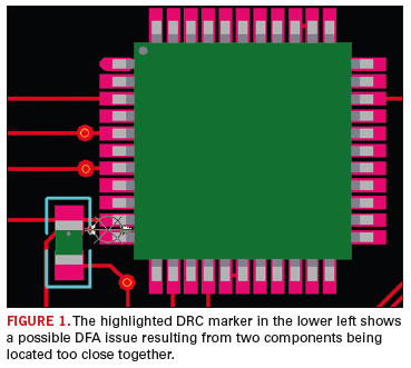
In FIGURE 1, a DRC marker is indicating a DfA issue where two components have been placed too close to each other. This may cause defects during the assembly process, due to manufacturing variation in the placement of these two components.

In more advanced scenarios, these DRC markers may also contain comments that were made by individual reviewers, possibly captured over multiple review cycles. When all analysis and review is completed, the information is communicated back to the designer for disposition. The designer now has accurate, unambiguous feedback to decide what corrective actions need to take place to improve the product design for manufacturing.
Design for Test
When performing DfT analysis, understanding the actual electrical test access points is critical. The external copper layers, solder mask layers, component outlines and net lists must all be available to accurately determine the actual electrical accessibility of the design, and correspondingly, to calculate the actual test coverage.The old rule-of-thumb of one test point per net is insufficient for the majority of today’s PCBs. If the board has some form of powered up test, additional test points that are separate from the measurement test points are required to apply this power to the board. If boundary scan is available on the board, certain nets may not even need a test point, as there may be enough test capability using the boundary scan cell. In this scenario, the net should indicate that it does not need a test point, and the DfT analysis adjusted automatically. Resistors, capacitors, and inductors may need additional test points on either side of the components for four-wire measurements that increase accuracy on certain types of value.
Once the test probe and corresponding alternate accessible locations have been finalized, they need to be communicated to manufacturing. This information becomes increasingly important for debugging test programs as well as repair. On large boards with incomplete silk screens, being able to quickly enter probe names listed on fault tickets and relate them to the corresponding nets can significantly decrease the mean-time-to-repair issue.
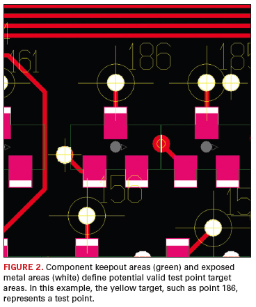
FIGURE 2 shows the result of the DfT analysis on an example board. The component outline in green is used as a keepout area for test probes. The white regions are exposed metal that are analyzed for valid test probe locations. If enough test regions are available for sufficient coverage, test probes can be placed, such as the yellow probe labeled 186.

Transitioning Design Data into Manufacturing
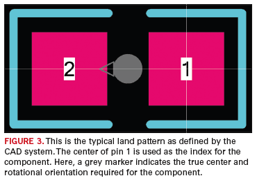
The physical design data is just one part of the information required to manufacture a printed circuit board. Another critical item is the production BOM data. As opposed to the design BOM, the production BOM represents exactly which version of a PCB design will be manufactured. The production BOM also typically comes from a separate business system within the company, not the design data. BOMs are typically an arbitrary file format that contains manufacturing relevant data such as where the actual components will be placed on the board and whether certain locations will not be populated.It is not possible to rely on the layout data directly to determine the pick up point and component rotation, as this might not have an accurate relation to the actual part. Manufacturing assembly machines need the center of the part as its pick up point, which isn’t always coincident with the origin of the CAD land pattern. Likewise for rotation, the CAD land pattern zero rotation may not match the part zero rotation, and so parts get placed with an incorrect orientation. Being able to consistently normalize part locations and rotations significantly reduces errors in production.
FIGURE 3 illustrates a typical land pattern as defined in a CAD system. In this case, the center of pin 1 defines the origin for the component, and therefore it is this point that is used as the component position locator in the layout. The grey centroid marker has been added to the data to indicate a normalized origin and rotation that can be used to calculate the correct board location in x-y coordinates.

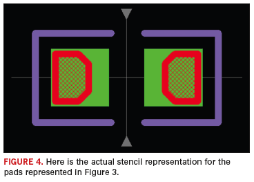
Typically, the paste layers in the CAD data are either a copy of the copper pads associated with a part, or are a simple reduction in size of the copper pads. This capability does not give enough flexibility to the stencil creation process to yield acceptable results. While these area reduction rules can work for some parts, more complex paste apertures are needed to create optimum solder goals. For example, notched rectangles or ‘home plate’ apertures are routinely used for two-pin chip components.
An example of a complex pad that has been defined for a stencil on a simple two-pin chip component appears in FIGURE 4. There is little relationship between the copper pads of the land pattern and the actual stencil pad required.

Summary
Neutralizing all the disparate source data into a single data format that can be used by manufacturing while eliminating redundancies is the key to accelerating design data from concept to manufacturing. This data can then be used as a collaboration medium between engineering, PCB layout, and manufacturing, balancing the unique requirements of each group and providing the ability to focus analysis and feedback, ensuring that the resultant product meets the quality and cost targets. These tools and the common data set provide the underlying method to communicate product-specific data from design to manufacturing, and will help manufacturers meet the increasing challenges they face in bringing products profitably to market. PCD&FMark Laing is product marketing manager for Mentor Graphics and can be reached at This email address is being protected from spambots. You need JavaScript enabled to view it..


