Signal Integrity Applications of Mathcad, Parts 1, 2 and 3

Mathcad is software with powerful capabilities to manipulate equations, numbers, text and graphs. The mathematical formulae and numerical values can be presented in an easy to read fashion. Mathcad allows graphics and text to be incorporated throughout the document, and if desired, the resultant files can be saved in HTML format for posting to a website.
Mathcad has proven invaluable for a wide range of engineering designs and can be used in some interesting signal integrity applications1,2,3. For example, Johnson et al1,4, presents Mathcad computations for DC copper resistance, capacitance of parallel plates, inductance of circular loops, coaxial cables, microstrip lines, and forward and inverse Fourier Transform (i.e., FFT and IFFT). Use of this software for Fourier transformations and square wave decomposition is also discussed by Brooks2, and application of Mathcad for simulating single-ended and differential pair high-speed topologies are demonstrated by Norte3.
As an example, let us apply Mathcad to analyze the asymmetric stripling configuration depicted by Figure 1. For asymmetric stripline (also referred to as offset stripline) the signal layer is sandwiched between two plane layers, but it is closer to one plane than the other (i.e., H1 not equal H). Setting H1=H leads to case of centered (or balanced) stripline.
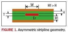
Figure 2 illustrates Mathcad calculations for characteristics impedance Z0 and propagation delay (Tpd). The parameters Er, H, H1 and W are defined at the top of Figure 2. The formulae for Z0 and Tpd are Equations 1 and 2, respectively.
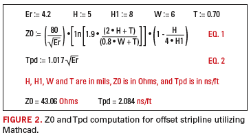
It illustrates that for Er = 4.2, H = 5 mils, H1 = 8mils, W = 6 mils and T = 0.7 mils, Z0 = 43.06 Ohms and Tpd = 2.084 ns/ft. In Mathcad files, parameter values can be easily altered to examine what happens to all variables and the graphs that depend on them. For example, setting Er = 4.0, H = 6 mil, H1 = 10 mil W = 5 mil T = 1.4 yields Z0 at 52.7 Ohms, and Tpd at 2.034 ns/ft.
The analytical technique for determining impedance is less accurate than using a field solver5. Yet an analytical approach provides an efficient means for Z0 computations and can furnish useful insight regarding effects of the various parameters that affect impedance.
Mathcad allows the incorporation of text, formulae, pictures, equations and graphs in the same document. This feature is demonstrated in the next example involving via inductance.
Every via has a parasitic capacitance and inductance. The via inductance is often more critical (to digital design) than its capacitance. The parasitic inductance associated with vias can degrade signal integrity6 and reduce effectiveness1 of the power supply bypass capacitors. Via inductance is also important in the analyses of power distribution network (PDN) since it increases the impedance between source and load7.
An example of calculating via (partial) inductance using Mathcad is illustrated below:
Equation for L(h) in Figure 3 is an accurate expression for an isolated via (distanced away from other vias).
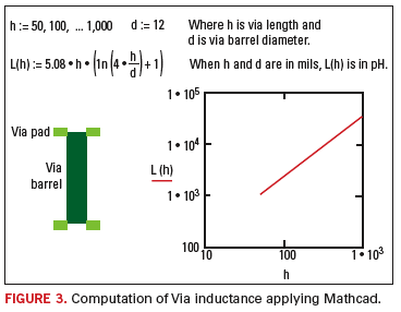
When there are other vias nearby, the mutual inductance must also be taken into account7.
Generally, Mathcad evaluates each statement in the program in sequence8, however, there are times when it is desirable to evaluate statements only when a particular condition is satisfied. This can be achieved by incorporating “if” statements.
As an example, the Serial Attached SCSI (SAS) channel insertion loss formula9 will be evaluated utilizing this Mathcad feature. Transmission line losses can affect the amplitude of high-speed signals and cause ISI5,10. Hence, when designing or testing a high-speed channel, it is crucial to consider the loss specifications.
For instance, the loss budget for PCI Express Gen1 is specified as 13.2 dB at a frequency of 1.25 GHz.
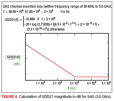
For SAS, the magnitude of insertion loss (SDD21) is given by a set of equations that can be analyzed using Mathcad as shown by Figure 4.
Above examples demonstrate that Mathcad offers powerful capabilities for analyzing and solving signal integrity problems. Additional mathematical SI applications will be explored in Part 2 of this article.
Mathcad offers efficiency and flexibility for solving mathematical equations.
It can treat analytical expressions having scalar (a single number), vector (column of numbers) and matrix (a rectangular array of number). An array is a general term for vector or matrix.
The Mathcad logarithmic features include ln(z) which returns the natural log of z (z ≠ 0) and log(z,b) which outputs the base b logarithm of z (z or b ≠ 0). If b is omitted, then log(z,b) equals the base 10 logarithm. Hence, log(z) returns the common logarithm of nonzero z.
Let us analyze, applying Mathcad, the concept of coupling even and odd mode impedances.
The electric and magnetic fields associated with coupled traces (i.e., traces located in close proximity) will interact in manners that depend on each line’s signal patterns. The effective characteristic impedance and velocity of the transmission will be altered due to such interactions. Figure 5 displays the computed (using HyperLynx from Mentor Graphics) odd and even electric (in blue) and magnetic (in red) field distributions for a coupled microstrip.
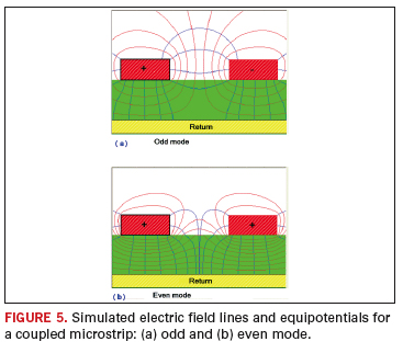
Two coupled traces excited by signals of equal magnitude but opposite polarity (180 degrees phase difference) will produce the odd-mode (also called differential). When these traces are driven by identically phased signals, then the even (or common) mode will result. The relationship between the characteristic impedance of each line Z0, the odd mode impedance Z0o and the even mode impedance Z0e is governed11 by:
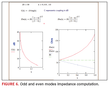
For any geometry, Z0o and Z0e depend on coupling equivalent magnitude of coupled energy depends on the odd and even mode impedances. Figure 6 presents impedance formulae for quarter wavelength matched lines solved with Mathcad.
As coupling intensifies, even mode impedance is likely to be high11 since the inductance increases and capacitance diminishes (because field lines are more concentrated between coupled traces and not at the common ground/return).
In a Z0 = 60 ohms system for weak coupling (such as k = 0.03) yields Z0e = 61.83 ohms and Z0o = 58.23 ohms. For a strongly coupled case (k = 0.7) with Z0 = 60 ohms outputs Z0e = 142.83 ohms and Z0o = 25.21 ohms. Thus when coupling is strong, Z0e and Z0o can significantly differ from Z0. Frequently, Z0o and Z0e for a coupled pair are plotted against trace separation12.
Such graphs reveal that Z0o and Z0e are close to Z0 when trace separation is large (which corresponds to weak coupling). However, when trace separation is small (resulting in strong coupling) there is a significant impedance difference.
When ascertaining the correct12 termination for a topology (in order to minimize reflections and maintain signal integrity) it is critical to take into consideration the even and odd mode impedance values.
As another example, let us apply Mathcad to a case of coplanar structure, which demonstrates this software’s capability to treat hyperbolic trigonometric such as Tanh( ) and special functions (such as ratios of complete elliptic integrals).
Coplanar waveguide (CPW) is a transmission line geometry that includes a central current-carrying trace on top of a dielectric substrate, with side grounds extending beyond a symmetric gap to either side of trace. There are several different types of CPW transmission lines including grounded CPW13 that has an additional ground below the substrate and ungrounded CPW (for which the side grounds coplanar to the signal trace provide the only return path).
CPW can have a lower loss tangent than microstrip (signals coupled mostly through air) and higher skin effect losses (fields concentrated on the edges of trace and grounds). CPW is generally defined by center strip width w, gap width g, substrate height h, and substrate dielectric material. Metal thickness t can be also important, especially when t ≥ 0.1w or t ≥ 0.1g.
The characteristic impedance Z0 of CPW can be controlled14 by varying the trace width, the spacing-to-ground, and the dielectric thickness or material.
Coplanar transmission line structures offer similar advantages to a microstrip in that signal is carried on an exposed surface trace where a surface mount component can be attached. However, unlike a microstrip, the CPW (at least in an ungrounded form) can have low parasitic losses between surface mounted components and an underlying ground plane. It is also possible to narrow the traces13 to match component pad widths while maintaining constant impedance.
CPW can also provide good inherent crosstalk immunity for two layer boards, because it is less sensitive to the
presence or absence of a backside of board ground plane.
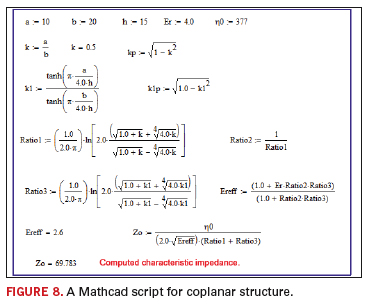
The primary disadvantage of CPW is that it is more difficult to design compared to microstrip or stripline. If the CPW’s aspect ratio (the ratio of gap to trace width) becomes too high or too low, parasitic modes can replace the desired CPW mode resulting in poor performance. Grounded coplanar geometry is depicted in Figure 7. A Mathcad script for computing the impedance of this type of coplanar structure is illustrated by Figure 8.
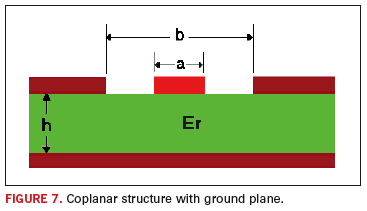
In Figures 7 and 8, a denotes trace width and b denotes the sum of trace width and separation, which is the same notation used in Wadell13. However, in many other publications the trace width is represented by w, and spacing to adjacent ground traces is given by s (or gap width g). In Figure 8, the expressions for Ratio1 and Ratio2 are called ratios of complete elliptic13 integrals of the first kind.
In signal integrity there arise certain quantities containing complex (real and imaginary) terms. For instance, permittivity of dielectric materials15 includes a real part (dielectric constant) and an imaginary part (loss). Another example of this is found in the impedance through a bypass capacitor16 that has a real part, the equivalent series resistance ESR, and an imaginary term, capacitive/inductive reactance. Determining these quantities can necessitate the use of complex algebra or calculus.
Mathcad accepts complex numbers17 of the form Re + (Im)i, where (Re) and (Im) represent ordinary numbers. Imaginary numbers may be followed by either i or j; however, Mathcad normally displays them followed by i where i equals the square root of negative 1. When typing complex numbers into a Mathcad formula, it is important to note that i or j alone cannot be used to represent the imaginary unit. Instead, it is necessary to type 1i or 1j, otherwise i or j will be interpreted as a variable. When the cursor is outside an equation having 1i or 1j, Mathcad will hide the superfluous 1.
Mathcad Applications to Single-ended and Differential Signal Propagation
Forward Fourier transform and its inverse furnish a means for data conversion from time to frequency domain and vice versa. Mathcad makes available two Fourier transform pairs: FFT/IFFT and CFFT/ICFFT. The former pair is applicable if the data values in the time domain are real and data vector has 2^m elements (m being an integer, m > 0). For all other cases, the CFFT/ICFFT pair is required. This is because, for real data, the second half of the transform is just the conjugate of the first. The FFT/IFFT takes advantage of this fact-saving memory and time (by discarding the second half of the result vector). The CFFT/ICFFT pair does not assume symmetry in the transform and should be used for complex valued data. The CFFT/ICFFT can be also employed for real numbers, which are just a subset of complex domain.
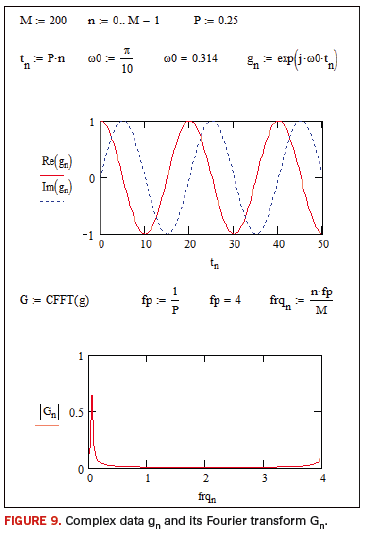
As an example, Figure 9 presents a complex time domain vector gn with real part [Re (gn)] and imaginary [Im (gn)]. There are M data points at sample spacing P (with reciprocal fp). n represents an index/integer and ω0 is angular frequency. tn and frqn are horizontal axes for time and frequency plots respectively. Mathcad CFFT is executed to generate the vector Gn in frequency space.
Furthermore, ICFFT can be operated on Gn to reproduce gn.
This implies the Fourier transform pair: G := CFFT(g) and g := ICFFT(G).
Fourier transform possesses remarkable applications in high-speed digital design. Digital signals can be approxi mated by square waves,18 having wide bandwidths or many frequency components. Fourier expansion can evaluate the spectral content (or harmonics) of such periodic time domain waveforms.
TDR measurements are related19 to corresponding VNA measurements via Fourier transform.
Another notable feature of Fourier transform is that convolution in time domain, often difficult to compute, is converted into a simple multiplication20 in frequency domain.
A discrete-time approximation to the Fourier transform called DFT forms a foundation for fundamental techniques and applications of digital signal processing (DSP).
Johnson, et al4 have simulated pulse propagation by applying Mathcad’s FFT/IFFT feature. Norte 3 has also illustrated Mathcad’s simulation of single-ended and differential high-speed topologies.
Consider the single-ended topology in Figure 10, which includes a driver U1, a transmission line T1 and a receiver U2. T1 has bandwidth (Bw) and characteristic impedance (Zo). U2 can be modeled by parasitic resistance (Rr) in series with capacitance (Cr).
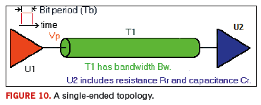
U1 outputs a series of pulses having bit period (Tb) and launches a voltage waveform (Vp) at input of T1. These signaling schemes can be simulated using various tools, including SPICE or SI tools from companies such as Mentor Graphics, Cadence, Ansoft and others. It can be also solved by Mathcad, which provides an economical21 approach for generating dependable results and design guidance.21
Application of Mathcad for simulating such single-ended signaling is demonstrated by Figures 11 and 12.
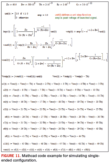
In Figure 11, Bw symbolizes the transmission line bandwidth in Hz. Zo equals line impedance (ohms). Tb represents the input pulse’s bit period in seconds. Rr is the load series resistance and Cr the load capacitance (Farad). Rr is usually on the order of milli-Ohms, and Cr includes C_comp and C_pkg.22
Figure 11 involves transmission of a series of bits across the interconnect. The data pattern is encoded with industry-standard non-return-to-zero (NRZ) format. In NRZ, the binary 1 and 0 are a positive and a negative square wave pulse respectively.
The uni(t) function aids in forming the NRZ bit waveform. The load impulse response ignoring propagation delay is impr(t). The vstp(t) models the transmission line as a first-order low-pass filter. The pulse waveform just before the receiver equals vstp(t) – vstp(t-Tb). The convolution integral of this waveform and impr(t) yields the output voltage Voutp(t), which is sectioned into Vout1(t) and Vout2(t). The difference Voutp(t) – Voutp(t-Tb), in turn, produces the received pulse Vrec(t). Finally, vnrz(t) is the NRZ 50-bit stream, which is expressed as summation s1(t) + s2(t)+… +s10(t).
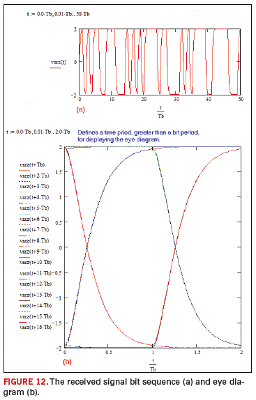
vnrz(t) as depicted by Figure 12a consists of :
10101100111000101010111101100001010111100111110001
An eye pattern at the receiver can be constructed via bit-by-bit superposition of the received bits.
Figure 12b shows an eye pattern formed by graphing 16 bits on the same graph. The plotted bits embrace vnrz(t+Tb), vnrz(t+2Tb), ……….vnrz(t+15Tb), vnrz(t+16Tb). Plotting several Y-axis expressions versus the same X-axis in Mathcad requires entering the first expression followed by a comma. A placeholder will then appear below the first expression. When the second expression is entered followed by a comma, another placeholder results for entering the next expression. This process can be repeated to graph multiple expressions.
Eye diagrams are frequently generated employing a large number of pseudorandom bit sequence (PRBS)23, such as a PRBS [(2^7) – 1]. However, eye patterns created by Mathcad based on a limited number such as 16 bits can be still valuable particularly for examining trends.21 For instance, it can be useful for analyzing effects on the eye pattern caused by variations in bandwidth or load capacitance. Trends based on 16 bits can be quite similar to those associated with a much greater number of signal bits.
As an example, decreasing the line bandwidth (Bw) (in Figure 11) from 500 MHz to 100 MHz will reveal degradation in eye opening of Figure 12b.
Consider a differential topology as displayed by Figure 13. It comprises a differential driver (U1), transmission lines (T1, T2, T3 and T4), termination resistor (Rt) and differential receiver U2. The concepts governing single-ended signaling can be extended to differential case, but it requires several important considerations.

Differential signaling involves propagation of signals on a pair of coupled transmission lines. The degree of coupling influences impedance, signal velocity (timing) and termination requirements.
The non-inverted signal Vp traveling on one line is the complement of an inverted signal Vn on the second line. For instance, if Vp is given by:
10101100111000101010111101100001010111100111110001
Then Vn having opposite polarity (each “1” is replaced with a “0” and vice versa) consists of:
0101001100011101010100001001111010100001100001110
The differential receiver acquires the difference Vp – Vn to ascertain the high or low state of the received signal. The reason for capturing the voltage difference is to minimize the common-mode noise. Mathcad scripts for treating differential topologies are described in Reference 3, found in Part 1 of this series.
In conclusion, Mathcad can be effectively applied for analyzing signal-integrity concepts, solving complex signal-integrity expressions and simulating high-speed PCB topologies. PCD&F
Dr. Abe (Abbas) Riazi is a senior staff electronic design scientist with Broadcom Corp. in Irvine, CA, and can be reached at This email address is being protected from spambots. You need JavaScript enabled to view it..
REFERENCES
Dr. Abe (Abbas) Riazi is a senior staff electronic design scientist with Broadcom Corp. in Irvine, CA and can be reached at This email address is being protected from spambots. You need JavaScript enabled to view it..
ACKNOWLEDGEMENTS
I am thankful to Mr. Mohammad Tabatabai of Broadcom Corporation.REFERENCES
1. Howard Johnson and Martin Graham, “High-Speed Digital Design: A Handbook of Black Magic”, Prentice Hall, 1993, PP. 258-260, PP. 409-439.
2. Douglas Brooks, “Signal Integrity Issues and Printed Circuit Board Design”, Prentice Hall, 2003, PP. 18-21.
3. David Norte, “ Learn Signal Integrity Design Principles With Mathcad”, The EMC, Signal and Power Integrity Institute, 2005, PP. 5-29, PP. 41-48.
4. Howard Johnson and Martin Graham, “ High-Speed Signal Propagation: Advanced Black Magic”, Prentice Hall, 2003, PP. 249-250.
5. Eric Bogatin, “Signal-Integrity Simplified” Prentice Hall, 2004, P. 257-262, PP. 334-335.
6. Stephen H. Hall, Garrett W. Hall, James A. McCall, “High-Speed Digital System Design A Handbook of Interconnect Theory and Design Practices”, John Wiley & Sons Inc., 2000, PP. 102-104.
7. Istvan Novak and Jason R. Miller, “ Frequency Domain Characterization of Power Distribution Networks”, Artech House Inc., 2007, PP. 43-54.
8. “Mathcad 2001 User’s Guide”, Math Soft Inc. 2001, P. 286
9. “Information technology – Serial Attached SCSI – 1.1 (SAS-1.1)”, Working Draft American National Standard, Project T10/1601-D, Revision 10, September 21, 2005, PP. 136-146.
10. Abe Riazi, “Timing Analysis Techniques for Digital PCBs,” Printed Circuit Design & Fab, February 2008, PP. 17-19.
11. “Even and odd mode impedances” Microwave Encyclopedia, 2006.
12. “Even mode impedance – an introduction”, Polar Instruments Ltd., Application Note AP157.
13. Brian C. Wadell, “Transmission Line Design Handbook”, 1991, Artech House, PP. 73-89, PP. 464-467.
14 . Rick Hartley, “RF / Microwave PC Board Design and Layout” L-3 Avionics Systems.
15. A. Kumar and S. Sharma, “Measurement of Dielectric Constant and Loss Factor of the Dielectric Material at Microwave Frequencies’, Progress in Electromagnetic Research, PIER 69, 47-54, 2007.
16. Douglas G. Brooks,” ESR and Bypass Capacitor Self Resonant Behavior How to Select Bypass Caps”, UltraCAD Design Inc., 2000.
17. Alan Felzer, “Introduction to Mathcad”, August 2003.
18. Stephen H. Hall, Garrett W. Hall and James A. McCall. “High-Speed Digital System Design, A Handbook of Interconnect Theory and Design Practices, John Wiley and Sons Inc., 2000, p. 85.
19. “TDR and VNA Measurement Primer” Application Note, 2004, TDA Systems Inc.
20. Zack Settel and Cort Lippe. “Real-Time Frequency-Domain Digital Signal Processing on the Desktop,” Proceedings of the 1998 International Computer Music Conference. San Francisco Music Association, pp. 142-149.
21. David Norte.“Transmission Line Discontinuity With a Series RC Load” www.the-signal-and-power-integrity-institute.com.
22. Abe Riazi. “Stub or no Stub?” Printed Circuit Design and Manufacture, October 2004, p. 18.
23. Chih-Kong Ken Yang, Ramin Farjad-Rad and Mark A. Horowitz. “A 0.5-um CMOS 4.0-Gbits/s Serial Link Transceiver with Data Recovery Using Oversampling,” IEEE Journal of Solid-State Circuits, vol. 33, no. 5, May 1998, pp. 713 - 722.


