What is Inductance?

A closed loop creates inductance, so control your signal path by minimizing the loop area.
While many of us feel that we understand inductance, in reality inductance1
is a commonly misunderstood concept. Inductance is important to EMI/EMC
and high-speed signal integrity (SI) design considerations since it is
one of the primary limiting factors in high-frequency design. Whenever
there is metal, and current flows though that metal, inductance is
present and will affect the current flow. At high frequencies, this
intrinsic inductance dominates all components, traces, and metal
planes. Capacitors and resistors too, become inductors at high
frequencies.
A complete study of inductance would
fill many volumes. The purpose of this article is to help the reader
better understand the concepts of inductance as it applies to
EMI/EMC/SI design, especially on printed circuit boards.
One
fundamental fact that is taught in first level electronic circuit class
is that the current must always return to its source. So, if there is
current flow, there must be a closed loop (so that the current can
return to its source). This closed loop of current creates inductance.
Electromagnetic Induction
When the current in a loop changes with respect to time, the magnetic field associated with that current also changes. As this changing magnetic field cuts through a conductor it induces a voltage in the circuit of that conductor. This occurs whether the magnetic field lines cut through a different conductor or the same conductor as the original current. The voltage induced in a single wire loop is equal to the time rate of change of magnetic flux passing through the wire loop.2 This is described in Faraday’s law of electromagnetic induction as:

While equations, such as Equation 1,
can look intimidating, when we dissect it to interpret the meaning of
the equations, it not only makes the concept clearer, but reduces the
intimidation factor. Consider the left hand side of Equation 1. This
shows an integration that is along a line that closes upon itself. The
electric field along that path, multiplied by the length of the path,
provides the voltage around this closed loop3. Now, let’s
consider the right hand side of Equation 1. We observe the double
integral, which is simply the area of a surface, and the amount of
time-varying magnetic flux contained within that surface area. Of
course, if we have a surface area, there must be a closed loop around
the circumference of the surface area. Note that on both sides of the
equation, a closed loop is required! The left hand side of Equation 1
shows the closed path as part of the integration and the right hand
side shows the closed path as the circumference of the area.
The
left hand side of Equation 1 gives the voltage around this close loop,
and the right hand side shows that this voltage will be negative! This
negative voltage will inhibit the original current that created the
magnetic flux, effectively providing impedance to the original current
flow.
Simple Rectangular Loop

![]()
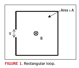
We can simplify the general case provided in Equation 1 to a simple rectangular loop as shown in Figure 1. If the loop is small compared to the wavelength of the frequency of interest, then it can be assumed that the magnetic flux is constant over the area A, and Equation 1 can be reduced to:
![]()
The
amount of voltage induced from a time-varying magnetic field can be
found for any geometry using Equation 1 and for a simple rectangular
loop using Equation 2.
Calculating Self Inductance
There
are a number of terms to describe inductance. Self-inductance and loop
inductance are the most common and mean the same thing. Recall from the
previous sections that induction occurs when a time-changing current
causes magnetic lines of flux to cut through metal conductors. Until
now, only the case where these lines of flux caused by a current in one
loop cut through the conductors of another loop was considered. These
lines of flux will also cut through the conductors of the original loop
as well. This gives rise to the loop’s self-inductance.
Isolated Circular Loop
The self-inductance of an isolated circular current loop in free space can be found using the fundamental relationship for mutual inductance if the two loops are considered to be overlapping. For a simple isolated current loop, where the wire radius r0 is much smaller than the loop’s radius a, then the loop’s self inductance is approximated as in 3,4:

If
multiple turns of the wire loop are used, then the inductance is simply
multiplied by the number of turns to find the total inductance of the
number of loops.
It is important to note that Equation 3
clearly shows that the value of the inductance will change quickly with
the loop area, and much more slowly with the conductor size. For
example, the loop area will dominate the amount of inductance, not the
trace width or thickness on a PCB.
Isolated Square Loop
For an isolated square loop in free space, the self-inductance can be found to be:

where
p = a/r0
a = length of side, and
r0 = wire radius.
Once again, note that Equation 4
clearly shows that the value of the inductance will change quickly with
the loop area, and much more slowly with the conductor size.
For the case where the wire radius is much smaller than the loop radius (r0 << a), Equation 4 reduces to:

Note that for these calculations of self-inductance the contribution by the internal flux within the conductor has been neglected. This term is most important at low frequencies when skin depth is not important and the current is uniformly distributed across the cross section of the conductor. For high frequencies, this term can be ignored. This self-inductance from the internal flux is given as a per-unit-length parameter as:

This term is then multiplied by the loop length to find the total contribution of the internal flux.
Isolated Rectangular Loop
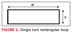
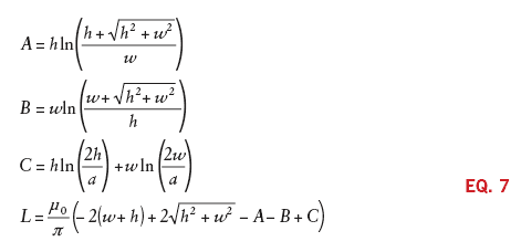
For a single turn rectangular loop in free space5, the self-inductance can be found from:

where
w = the width of the rectangle (wide dimension)
h = the height of the rectangle (short dimension), and
a = the wire radius.
Once again, note that Equation 7
clearly shows that the value of the inductance will change quickly with
the loop area, and much more slowly with the conductor size.
Inductance of a Via
There
is no such thing as inductance of a via by itself. Somehow, the return
path must be considered. In the case of a PCB via, the intentional
signal current flows on the via, and then must return. If there is a
return via close to the signal via, the amount of loop area, and
therefore the inductance, will be small. However, as the return via
moves further away from the signal via, then the loop area (and
inductance) grows quickly. Eventually, the return via is no longer used
for any significant amount of return current, and all the return
current flows though the dielectric displacement current (and the
return via has no impact in the inductance the signal experiences). As
the return via moves further away the return current spreads out in all
directions in order to use the dielectric displacement current. This
current spread provides many more opportunities to couple onto other
signal vias and cause noise problems for other signals.
Summary
The
concept of inductance only has meaning when the entire loop is
considered. A wire that does not form a loop will have no inductance
since there can be no current flow. When calculating inductance, the
loop area will dominate the value of inductance. Conductor thickness
plays a minor role. So PCB designers can have a greater influence on
their signal path (including the return current path) by minimizing
this loop area. PCD&F
References
1.
Oliver Heavyside first coined the term ‘inductance’ in 1886. He also
created the terms ‘capacitance’ and ‘impedance’. Source: D. Johnson, J.
Johnson and J. Hilborn, Electric Circuit Analysis, Prentice-Hall, 1989.
2. The basic definition of voltage is the electric field multiplied by the distance.
3. J.D. Kraus and K.R. Carver, Electromagnetics, 2nd Edition, McGraw-Hill, 1973.
4. A.E. Ruehli, “Inductance Calculations in a Complex Integrated
Circuit Environment,” IBM J. Research and Development, 16, pp 470-481,
1972.
5. F.W. Gover, Inductance Calculations, Dover Publications, NY, 1946.
Dr. Bruce Archambeault is a IBM Distinguished Engineer and IEEE Fellow. He can be reached at This email address is being protected from spambots. You need JavaScript enabled to view it..


