Solve Design Problems with Signal Integrity Optimization
Optimization routines save time by using automated methods to determine if performance goals are met.
Printed circuit board (PCB) design often begins with the development
of signal integrity (SI) guidelines to ensure adequate performance of
the final product. Most often the guidelines are based on traditional
engineering practices through manual manipulation of circuit parameters
and judicious interpretation of results. While such approaches do
result in useful conclusions, they can also consume significant effort,
only to reach sub-optimal conclusions. Alternatively, optimization
routines can be used to aid in SI analysis and the development of PCB
design guidelines.
Optimization routines have been
well proven to aid analysis across a variety of common tasks, such as
determining the optimal values for circuit parameters. In addition,
there are several non-traditional applications where optimization can
be useful, such as developing application-specific termination schemes.
With increasingly higher speeds and routing
densities, proper signal integrity (SI) engineering is an important
aspect of printed circuit board (PCB) design. At its basic levels, SI
engineering involves the development of design guidelines for impedance
control, termination, attenuation, and isolation. As design complexity
increases, so does the associated SI analysis.
Where
feasible, common industry practice (i.e., rules of thumb) can guide SI
analysis on many issues with good results. In situations where more
significant analysis is necessary, SI engineers can potentially benefit
from non-traditional approaches. Optimization routines are engineering
tools that are often useful in these situations, as they automate the
process of tuning parametric values to achieve desired performance.
One of the more common applications of optimization routines is the development of equivalent-circuit models1,2
of various passive interconnect. In these cases, the interconnect
performance is measured in the lab in either time or frequency domains.
Based on the measured performance and knowledge of the physical
structure, a circuit topology is generated to approximate the
performance. Optimization is then used to adjust the various circuit
element values to best approximate the measured performance. In
addition to model development, optimization routines are also commonly
used for obtaining peak performance of completed links, such as
determining optimal termination resistance.
Beyond these common applications, there are several non-traditional applications of optimization routines3
that can be of similar value. For example, it is often possible to use
optimization routines to assist in developing unique circuit
architectures or to optimize cost versus performance trade-offs.
Optimization Basics
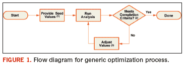
Optimization routines rely on an iterative process similar to that shown in Figure 1.
For SI analysis, the process generally starts with a circuit model that
has undesired simulated performance. Within the circuit model, a
specific set of user-defined circuit parameters are selected, and these
parameters are allowed to vary within a specified range. The parameters
can be typical circuit values such as resistance and capacitance, or
they can represent other physical quantities such as geometric length
or dielectric constant. When the first simulation is run, these
variable parameters are given user-defined seed values (Note 1 in
Figure 1).
When the first
simulation iteration is complete, the circuit performance is compared
to the desired results using a set of user-defined metrics (Note 2 in
Figure 1). The metrics can be simple, involving single-point values
such as a specified voltage at a circuit node, or they can consist of
complex functions such as relative match of two waveforms over time. If
the simulated performance falls within a specified tolerance of the
desired performance, then the optimization routine is complete and
returns the original seed values.
If the simulated
performance does not match the desired performance, then the internal
optimization algorithm considers the previous results and calculates
new values for the circuit’s variable parameters (Note 3 in Figure 1).
Using the new values, the simulation is run again, the new simulated
results are compared with the desired results, and the iterative
process continues until the desired performance is obtained. The output
of the process is the parametric values that allow the circuit
performance to meet completion criteria.
The
advantage in using optimization routines comes from the algorithm that
calculates new values for the circuit’s variable parameters. Typically,
these routines can adjust many variables simultaneously with fast
convergence to an optimal operating point. Over the years, numerous
algorithms have been developed4-10, and each has its own
respective strengths and weaknesses, the detailed discussion of which
is beyond the scope of this article.
Challenge: Multi-Drop Bus
Optimization
routines can be of significant help in many unexpected ways, one of
which is aiding in the development of application-specific termination
schemes. To provide an example of such an application, this section
describes the process of using optimization routines to solve a common
design challenge – the desire to increase effective memory depth
without increasing pin count or routing density – accomplished by
sharing address and data busses between multiple memory chips.
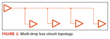
As shown in Figure 2,
the associated net topology is called a multi-drop bus. Here, a single
output buffer (often a processor ASIC) drives a trace with multiple
stubs branching off the main trace with each stub having its own load
device (memory chip). From an SI perspective, the challenges with this
circuit topology include termination of each interconnect path,
potential over-loading of the driver, and constructive/destructive
interference from multiple reflections.
A
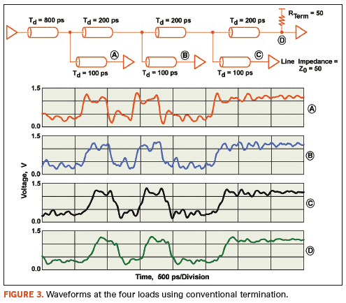
common termination approach for such a topology is simply to terminate
the far end of the primary signal path with a 50-Ohm termination
resistor to VTT. While such a termination scheme works well for simple
point-to-point circuit topologies, the signal waveforms shown in Figure 3
clearly demonstrate the undesired effects of inappropriately using this
design practice in a situation that requires more analysis.
In
this example based on 1.5-V HSTL signals, the signals collapse to
levels within 90 mV of the 750-mV reference voltage, less than the
200-mV HSTL specification11 for AC conditions. Accordingly, the design
needs to be changed for it to be reliably used in system applications.
The difficulty here is in trying to determine what alternative circuit
topologies to consider, and to then determine the appropriate values
for each circuit element.
To obtain adequate SI
performance in a multi-drop net such as this, there are numerous
termination options whereby termination resistors are placed in shunt
and/or series at various circuit nodes. However, the proper location
and value of the termination resistors is not readily apparent, and it
would take significant time and effort to manually explore all possible
options.
Alternatively, we can use optimization
routines to aid in determining proper termination architecture and
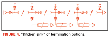
associated resistor values. The process starts by tossing a veritable
“kitchen sink” of termination options at the problem, as shown in Figure 4, where termination resistors are placed at each and every node, in both shunt and series configurations.
The
process then uses optimization routines on the “kitchen sink” circuit,
and the resulting parasitic values are inspected. If any parasitic
value falls outside a useful range, the entire element is removed from
the circuit, and optimization is performed again. The process continues
until all parasitic values approach reasonable and practical values and
the resulting signal integrity is adequate.
One
common feature most optimization routines share is a decreased
efficiency with an increase in the number of variables. If all twelve
resistors and all seven line impedances in the above example were
allowed to vary independently, the optimization process would take
considerable time and the results could be impractical to implement.
Alternatively, it is reasonable to constrain the primary path from the
driver to the last receiver to one common line impedance, while all the
stubs rely on different impedances. Similarly, the three resistors at
each transmission line split can be chosen to be the same value as
those on the other splits, thus further reducing the number of
variables.
With most optimization routines, seed
and limit values are needed. For the transmission lines, a 50-Ohm
impedance is most-often used and will be the suggested nominal value
for the simulations. For the limits, practical values are chosen to
range from 25 Ohm to 100 Ohm. For the shunt resistors, nominal 50 Ohm
values are chosen with limits of 1 Ohm and 1,000 Ohm. For the series
resistors, 10 Ohm nominal, 1 Ohm minimum, and 1000 Ohm maximum values
are chosen. For all resistors, values approaching 1 Ohm will be
considered shorts and values approach 1,000 Ohm will be considered
opens. In all, the nineteen possible variables are reduced to eight.
Using
the circuit topology of Figure 4 and the parametric values discussed
above, optimization is performed with a goal of maximizing the eye
opening at all four loads. The results of the first optimization step
indicates that the circuit performed best when the source-series
resistor at the driver was 1 Ohm, which is at the bottom limit. In
addition, the intermediate series terminators along the primary
transmission path provide best performance when they have low values.
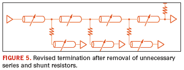
Accordingly, we can effectively remove these circuit elements by
replacing them with direct shorts. Similarly, the shunt resistor values
at the driver and along the primary signal path are sufficiently high
that we consider them to be opens, and thus remove them from the
circuit. The resulting circuit is shown in Figure 5, which is now much more practical to implement.
Using
the revised circuit, optimization is performed again to fine-tune the
remaining parasitic values. We then round off the results to practical
values, and the resulting circuit performance is shown in Figure 6.
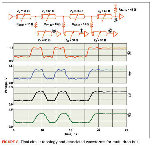
The
original non-optimized circuit produced poor signal waveforms with an
eye opening of just 90 mV beyond the reference voltage and failed to
meet the HSTL specification. Through the demonstrated iterative
optimization process, the eye opening improved to over 300 mV, the
signal quality improved dramatically, and the signals now exceed the
HSTL specification by 100 mV.
In addition to
determining reasonable parasitic values for the termination resistors,
optimization routines also aided in the development of the
application-specific termination architecture. Where it could have
taken hundreds or even thousands of simulations and many weeks of
hands-on time using traditional manual approaches to produce the same
results, the use of optimization routines in this case reduced the
number of manual steps down to three and reduced the hands-on effort to
a few hours.
Conclusions
Judicious
use of optimization routines can save significant effort using
automated methods to determine appropriate values to meet specific
user-defined performance goals, subject to constraints. In addition,
optimization can be of tremendous help in determining appropriate
circuit topologies for both models and circuits, and can often be used
to navigate through the various conflicting goals of cost, reliability,
and performance.
Optimization should be used with
caution, because issues such as non-convergence and inappropriate
results can occur. Therefore, it is imperative that all results are
validated, and it is recommended that users familiarize themselves with
all optimization options prior to using this procedure. PCD&F
REFERENCES
1.
Nimmagadda, S., A. Moncayo, and J. Dillon. Measurement, Modeling and
Simulation of a High Speed Digital System Using VNA and HSPICE.
Northcon. 1996. Seattle, WA: IEEE.
2. Huang, C.-C., et al.
Extraction of accurate package models from VNA measurements. in
Electronics Manufacturing Technology Symposium. 2000. Santa Clara, CA:
IEEE.
3. Zabinski, P., B. Buhrow, B. Gilbert, and E. Daniel, Application of
Optimization Routines in Signal Integrity Analysis, DesignCon 2007,
Santa Clara, CA, January 29 to February 1, 2007.
4. Yun, I. and G.S. May. Passive Circuit Model Parameter Extraction
Using Genetic Algorithms. in 1999 Electronic Components and Technology
Conference. 1999. San Diego, CA: IEEE.
5. Levenberg-Marquardt Algorith, http://en.wikipedia.org/wiki/Levenberg-Marquardt_algorithm
6. Ananth Ranganathan, The Levenberg-Marquardt Algorithm, cc.gatech.edu/people/home/ananth/docs/lmtut.pdf, June 2004.
7. Fletcher, R., Practical Methods of Optimization, NY, Wiley, 1993.
8. Gill, P.E., Murray, W. and Wright, M.H., Practical Optimization, Academic Press, London, 1981.
9. Levenberg, K. ”A method for the solution of certain problems in least squares,” Quart. Appl. Math., 2, 164-168, 1944.
10. Marquardt, D. ”An algorithm for least-squares estimation of
nonlinear parameters,” SIAM J. Appl. Math., 11, 431-441, 1963.
11. High Speed Transceiver Logic (HSTL): A 1.5 V Output Buffer Supply
Voltage Based Interface Standard for Digital Integrated Circuits. 1995,
Electronic Industries Association.
12. 72Mb M-die DDRII SRAM Specification, 2006, Samsung.
Pat Zabinski is a principal engineer, Ben Buhrow is a senior engineer, Barry K. Gilbert is director of the special-purpose processor development group and Erik S. Daniel is deputy director of the special-purpose processor development group, all at the Mayo Clinic; This email address is being protected from spambots. You need JavaScript enabled to view it..


