Troubleshooting the Innerlayer Process
Identifying and maintaining proper process controls is key to improving innerlayer yields.
An improved awareness of the relationship between key innerlayer
process controls and defect modes can help improve both product yields
and overall quality. Whether the process is designed to produce
ultra-fine line product or more mainstream innerlayers, each of the
steps within the manufacturing process can influence both quality and
yield. Identifying and maintaining the proper controls and procedures
for each process step is a critical first step to maintain high quality
while meeting cost targets. This review of the issues associated with
the liquid-resist based innerlayer process will provide an overview of
the critical issues.

Material Preparation and Handling
The
quality of the copper surface over which the resist is being applied
has a primary impact on the process defect level. In general, while
liquid resists have a better ability to cover surface defects, dents,
scratches or burrs on the copper surface, the surface condition can
still lead to formation of defects after etching (predominantly opens).
The key to avoiding such issues is to be aware of
the different points at which the copper surface can be damaged.
Control of the process starts with clear acceptance criteria for
incoming copper clad laminate. This should be combined with appropriate
levels of sampling and inspection to confirm that quality targets are
being maintained.
Each time clad laminate is
handled, there is another opportunity for creation of surface damage.
Both procedures and equipment maintenance schedules for sheet cutting
and edge cleaning operations should be examined to ensure that surface
quality is maintained.
Debris formed in these
operations is a primary source of contamination in the later resist
coating and exposure processes. Using clearly defined work practices to
eliminate debris at the source is the most effective approach to
avoiding problems in later process steps.
Scratch and burr defects are more easily formed on RTF foil, so particular care should be taken when handling these materials.

Surface Pre-Cleaning
Proper pre-cleaning is the key to achieving good adhesion between resist and copper.
The
typical process flow employs a cleaning step, followed by a copper
microetch and acid rinse. Usual process controls including cleaning
uniformity, using such tests as water break, and maintaining bath
concentrations and microetch rates based on measurements made at least
once per shift are always appropriate. More sophisticated techniques
such as contact angle measurement may be useful for troubleshooting
purposes, but are less suitable for routine use. Since variations in
copper foil grain structure can affect microetch rate, it is important
to ensure that coupons used to test etch rate are representative of the
product being run in the line.
Cases are
occasionally encountered when the preparation of a new cleaner bath led
to a significant improvement in resist adhesion, even though the water
break test showed no indication of insufficient cleaning. When
qualifying a line, data can be obtained to establish a defined dump
schedule for the cleaner, based on resist adhesion as a function of
cleaner bath age or throughput.
Whether the microetch
used is a persulfate or peroxide based material, creation of a
consistently rough surface morphology is required. Troubleshooting can
be done by correlating the surface condition (using a combination of
SEM and profilometry) with the data for resist adhesion after multiple
passes through the subsequent development process.
Liquid Resist Coating and Drying
Maintaining
the cleanliness of the environment used for the coating and drying
steps is critical. When troubleshooting yield loss, examination of the
resist layer after coating and drying can provide information on the
nature and source of particulate contaminants.
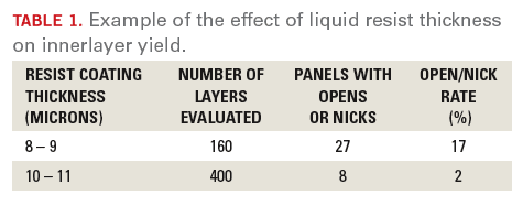
While
10 +/- 2 µm is often described as being the desired coating thickness
range for liquid resists – depending on the process control and
technology complexity level for an individual customer – the use of 8
to 9 µm coatings may not always provide acceptable yield.
Using
this approach to obtain initial baseline data for process capability,
and updating that information when a higher difficulty product is
introduced, will ensure that the best balance of performance and cost
is achieved.
Over or under drying a liquid resist can
lead to a variety of issues. Under drying may lead to defects
associated with damage during handling and stacking, loss of resist
adhesion, and changes in resist exposure and development properties
(such as excessive photospeed or formation of a negative or positive
resist foot). In contrast, overdrying can lead to loss of photospeed
and difficulty in achieving proper development. Sublimation of resist
components can also be an issue if drying is too severe, leading to
issues of debris build-up within the equipment.
Resist Exposure
Although
collimated sources (in which the light radiation from the source
follows a parallel path) may be used, non-collimated equipment is the
norm for liquid resist exposure. The combination of higher exposure
sensitivity of liquid resists with a collimated exposure source leads
to an increased sensitivity to particulate contamination, with
increased open/nick defects and lowered yields. Therefore the use of
non-collimated light is much preferred. The equipment used must be
capable of delivering sufficient light energy in an exposure duration
that results in an acceptable production throughput.
Enough
exposure energy must be provided to allow the resist to be fully
crosslinked, but excess energy will lead to lateral growth of the
exposed area, with a consequent loss of resist line width control.
Optimum exposure energy for a particular resist may be identified using
a Stouffer Step tablet1.
Since the artwork
must be tightly held against the resist-coated substrate, insufficient
delay time between vacuum application and exposure can adversely affect
resolution. To confirm proper settings, evaluate resolution as a
function of vacuum delay time. Artwork damage and contamination is also
an ever-present concern. Repeating defects appearing at the same
location on a panel is an indication of this issue.
Resist Development
The
developer process is required to remove unexposed resist (for a
negative resist) so as to allow an accurate transfer of the image from
the artwork to the final etched panel.
Residual
resist left in areas that were intended to be completely cleared will
prevent the subsequent etch step from properly removing copper from
those locations.
Issues of this type may be
associated with deficiencies in control of developer concentration or
temperature, failure to ensure that horizontal equipment is properly
maintained, for example, blocked spray nozzles or contamination of
transport rollers.
Even if the developer chemistry
and equipment is properly maintained, inadequate time, temperature,
water cleanliness or spray pressure in the post-develop rinse step may
also lead to residuals being left on the panel surface.
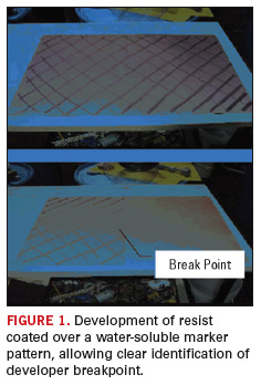
Optimum
developer speed is established using breakpoint testing, where
breakpoint is defined as the point at which the unexposed resist is
first washed away, revealing the copper substrate. Breakpoint should
take place sufficiently early in the developer chamber that complete
pattern formation is guaranteed, with no residual material remaining,
but not so early that resist feature line width is reduced by
dissolution in the developer chemistry.
While the exact breakpoint settings used in different processes vary, typical values range from 30% to 60%.
Etching and Resist Stripping
Proper
control of etch rate and etching factor is achieved through a
combination of chemical concentration management and equipment
maintenance. For most etching, temperature and spray pressure far
outweigh any other factors in determining etch rate.
Although
resist stripping does not directly affect the pattern formation, it may
sometimes have an indirect impact on process yield. Incomplete
stripping or copper surface oxidation after stripping can lead to a
non-uniform surface appearance. When finished innerlayers are examined
by AOI, these surface irregularities can trigger false defects. If the
equipment settings are adjusted to eliminate the false signals, AOI may
fail to detect actual defects, leading to scrapped panels at final, a
very expensive and undesirable problem.
Adhesion Promotion
As
global assembly has shifted towards lead-free processes, and with more
complex product often requiring multiple laminate operations, the
increased stresses placed on the innerlayer copper/laminate interface
have in many cases exceeded the capability of existing laminate
materials. Even when new materials designed for lead-free assembly
processes are used, unexpected failure modes can require the
re-evaluation of material qualification and test methods.
As
an example, delamination failures of boards have been reported in
assembly after storage in ambient conditions for 3 to 6 months. Prior
to lead-free, storage for this period of time would not have been
considered a potential problem. For these applications, some laminate
systems based on dicy cure have been found to not perform as well as
novolac systems.
In addition, surprisingly complex interactions between adhesion promotion systems and laminate material formulation have been reported for oxide, reduced oxide and oxide replacement. This has led to new approaches to adhesion promotion process qualification, including evaluation of adhesion performance on a wider range of copper substrates, and use of more severe screening tests.
Test combinations must certainly include copper foil
and plated copper (as would be seen on plated innerlayer products)
combined with the full range of laminate material types that will be
processed. Performance tests should include assembly simulation testing
immediately after lamination, after pressure cooker exposure and also
after extended room temperature storage. PCD&F
REFERENCES
1. Stouffer Industries, Inc. Step Tablet at stouffer.net.
Simon Lee is Regional Marketing Manager Imaging and Final Finishes – Rohm and Haas Electronic Materials Asia Ltd.; This email address is being protected from spambots. You need JavaScript enabled to view it.. Betty T.Y. Xie is Product Manager Imaging – Rohm and Haas Electronic Materials Dongguan Ltd.; This email address is being protected from spambots. You need JavaScript enabled to view it..


