Laser Direct Imaging Made Easy
With over 400 installations worldwide, LDI is gaining global market acceptance.
Laser direct imaging (LDI) technology for PCB applications is over
30 years old, yet, it is less than a decade since the technology became
a production proven tool. Today, there are over 400 units installed
worldwide. The reasons why it took so long to develop this installed
user base are many and varied, including technical hurdles such as
laser technology itself, computing power, availability of dry film /
liquid resists, optics, the art of combining these technologies, as
well as cost and the ability to support customers.
During
that time, many articles were written and presentations made on all the
wonderful benefits LDI brings to the PCB manufacturing process, such as
no photo-tool printing, faster turnaround for small jobs, tighter
accuracy, dynamic scaling functions, and high depth-of-focus.
There
is another side of the LDI that is often overlooked; that is, the
simplicity of the LDI solution. To penetrate the imaging market, the
suppliers of LDI equipment have developed a series of features that
enable both performance to specifications, and ease of use. Using the
feedback from numerous LDI customers, the systems have been improved.
The features of LDI equipment today make it an easier option for a PCB
manufacturer to implement, and because the process is digital, it is
easier to use than conventional imaging ever will be.
Once
the LDI users realized the advantages and potential for the technology,
they challenged LDI suppliers with requests and ideas that, in essence,
established the basis for process improvements.
What makes an LDI system easy to use? There are 4 groups of features that highlight the LDI’s general ease-of-use. They are:
- Process compatibility. LDI fits into your current process with minimal or no changes
- User interface. LDI allows you to be up and running in minimal time
- Image registration. LDI is compatible with many different target types
- Process feedback. LDI provides instant feedback on registration and other useful statistical data
Process Compatibility
UV-based
LDI systems will work with the same conventional resists as do
conventional exposure systems. The entire process has become simplified
through the removal of the photo-tool. Other than that, no change is
required. There are also faster, more sensitive LDI resists available
that can be used. The choice is left with the users based on their
process requirements and resist cost targets.
The
beauty of a digital system is that almost any combination of scaling
can be implemented. The options run the gamut from fixed scaling
(similar to contact exposure, where only one scaling factor is used for
the whole batch), through iterative, corrective mechanisms (where the
optimum scaling is converged upon, as the batch is being printed), to
global scaling systems (where each panel receives the best scaling
factor applicable to that particular panel).
Both
primary imaging and solder mask can be imaged using the LDI system.
There are several companies who have introduced faster solder resist
inks to the market in the past two years. This choice would be optimal
from the point of view of scaling accuracy, but some PCB fabricators
may be reluctant to introduce the LDI in the solder mask area, either
because it involves another equipment purchase, or because they need
their customer’s approval to make a material change.
Until
LDI is used in the solder mask area, the PCB fabricator can continue to
use the LDI for inner and outer layer imaging, even with global
scaling. Since you cannot have one photo-tool for each individual
panel, the next best solution is to use the minimal number of
photo-tools for the solder mask process, and still keep the design
specification on the annular ring.
There is special
optimization software that allows you to compute the minimum number of
groups that can be used to divide panels, allowing you to keep the
desired annular ring accuracy. Shown in Figure 1, the process is outlined below.

1.
The outer layer is exposed using LDI with global scaling. The scaling
factor used for the imaging of each panel is recorded in the log of the
LDI system.
2. After the outer layer process is finished and the
next (solder mask or conformal mask) process begins, the system log,
which includes the X- and Y-scaling factors for each panel, is fed into
the optimization application. In addition, the desired annular ring, or
hole-to-pad misalignment, is input into the application.
3. The optimization software tool then calculates:
- The number of films that should be prepared for plotting, for the next (solder mask or conformal mask) stage
- The scale factors for each individual film
- The sorting of panels to their specific group (or photo-tool).
The
user can then sort the panels into the number of groups (or
photo-tools) given by the optimization application, and continue with
the solder mask (or other post-process) stage with the desired accuracy
using the minimum number of photo-tools. If the PCB fabricator uses
serial number stamps, they will be able to sort panel groups according
to the stamp.
4. Since the scaling factors are
already known, there is no need to measure the panels again in order to
get the correct scaling factor for the plotter. This saves additional
time, and reduces process complexity.
5. The LDI
system can also be used to image the scaled data on a UV film, thus
saving several process steps. This is not a primary LDI use, but in a
few cases it could help get the best photo-tool in the first shot.
The
same software can be used for conformal mask before the mechanical
drilling step. All of the previously listed benefits holds true for the
conformal mask step as well. If the customer employs conformal mask
printing using the LDI, then the optimization application will generate
the optimal number of scaling factors to be used in the mechanical
drilling step.
Not only is LDI compatible with your
existing process, it can also be used to improve the process. There is
a vast amount of imaging data stored on the LDI system that can be used
to make improvements in other manufacturing processes.
User Interface
Using
customer feedback has allowed for the improvement of the user interface
to the point where ease-of-use alone has become a valid reason for
using LDI in the PCB fabrication process.
There is an intuitive graphical user interface, simple to operate and learn. An example is shown in Figure 2.
The short learning curve for the equipment is seen as a necessary
attribute. There is a strong focus on simple operational use. You can
have full control of multiple LDI systems on a single display. This
also allows fast and easy recall of previous fabrication work.
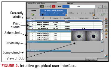
The user interface has been designed for a quick and easy setup of new work. It is only a matter of minutes to go from the CAM data to the start of imaging. Since job preparation is done in parallel to production, it allows for high system utilization. Only minimal inputs are required from the operator (e.g. panel thickness and energy in mJ/cm2) but it is also very easy to change working parameters directly on the screen.
The user interface also allows flexibility on
how panel sides are imaged, either side A followed by side B for each
panel (ABAB), or all the “side As” first, followed by “side Bs” (AABB).
All these functions can also be controlled from an off-line
application, outside of the yellow room environment.
Image Registration
For
image registration, the LDI system relies on acquiring target images on
the panel. This real time image acquisition and analysis process is
crucial for registration. Some LDI systems are compatible with a large
number of different target types, and have the capability to define and
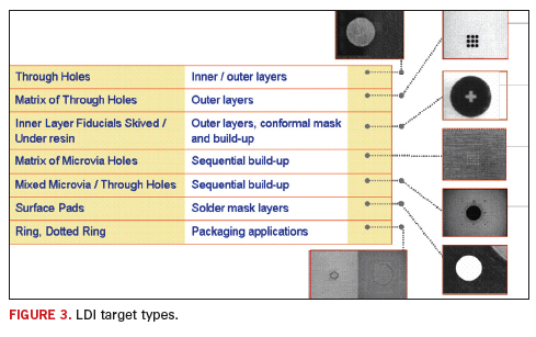
add as many targets as you like. The types of targets that LDI must be
able to incorporate are shown in Figure 3. These
targets include, through holes, matrix of through holes, innerlayer
fiducials skived /under resin, matrix of microvia holes, mixed microvia
/ through holes, surface pads, ring/dotted ring – all covered or not
covered by resist.
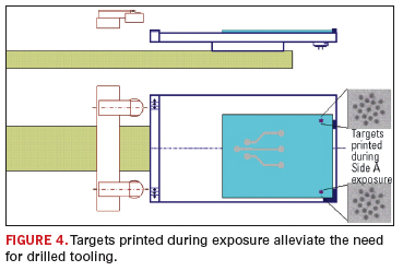
Some LDI systems use a UV marker to create targets on one side of an inner layer (Figure 4),
thereby avoiding the need for drilling through holes, which is an
additional undesirable process step. As one side of the innerlayer is
being printed, two UV marks are printed on the underside as well. When
the layer is turned over, those two UV marks are then used to achieve
accurate (or “the most accurate”) side-to-side registration.
Process Feedback
An
important aspect of every digital printing process is the availability
of instant feedback for the user. The quick manner in which data is
converted to imaged pattern must be accompanied by safeguards in the
form of alerts. For example, if the panel is badly distorted and the
dynamic scaling option suggests a value beyond the set limits, an alert
should appear. Another confidence building feature is the registration
feedback, essentially showing the operator the expected front-to-back
registration for the imaged panel.
In addition to
instant feedback, data can be generated from the LDI system’s vast
database of imaging history for review by supervisors and managers.
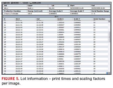
Since every image’s parameters are stored in the system, many
statistical charts can be easily and quickly extracted. These include
panels imaged over a specific period of time, panels per shift,
potential vs. actual panels per day, printed panels per energy setting
(mJ/cm2), system utilization (hours/day), average batch
size, panel size distribution, and much more. All of this information
can be accessed and customized for each PCB fabricator’s needs. This is
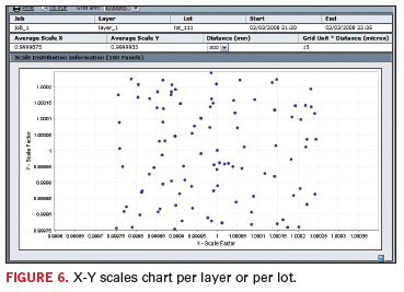
an example of the power of digital printing. The two examples, Figure 5 and Figure 6, show scaling data with respect to a particular batch.
Summary
In
the last few years we have witnessed the introduction of many new LDI
capabilities and uses. It is our prediction that LDI technology will
continue to proliferate. In addition to higher LDI speeds and increased
accuracy, there has also been an improvement in the cost of ownership.
New LDI capabilities are being developed, such as real time analysis,
advanced alert mechanism, on-line inspection and enhanced real time
feedback. The trend is a focus on improvements to productivity. It is
up to the many users of LDI to share their experiences with suppliers
and engage them in the development of future solutions. PCD&F
Guy Alon is the director of PCB marketing for Orbotech Inc; This email address is being protected from spambots. You need JavaScript enabled to view it.. Ralph Birnbaum, PhD is the LDI marketing manager of the PCB Division in Orbotech Ltd; This email address is being protected from spambots. You need JavaScript enabled to view it..


