Implementation of Buried Capacitance in High-Speed Designs
Embedded capacitance frees up the board surface for routing traces, can reduce the overall board size and can speed time to market.
The integration of embedded capacitor technology is driven by the
need to save board area and/or reduce board size, increase
functionality, lower costs and improve electrical performance. It has
been demonstrated that the performance of embedded capacitance laminate
layers in a PCB stack up are more effective in high-frequency noise
suppression than discrete surface mount technology (SMT) capacitors.
There is however, little information regarding the number of discrete
capacitors that can be safely removed by utilizing this technology.
As
other applications for incorporating embedded capacitance layers are
being examined (such as the modules used in cell phones and laptop PCs)
the ability to predict the number of discrete decoupling capacitor
components that can be safely removed is likely to be critical in the
decision of whether or not to use the technology. One approach to
determine this is to use the electrical performance simulation of
boards with and without embedded capacitors. To further the knowledge
in this area, additional data should be generated. The number of
discrete components that the model predicts needs to be compared to
those that can actually be removed from the board without a negative
impact. With a good predictive model, the decision to utilize embedded
capacitors can be simplified.
Redesigning with Embedded Capacitance
To
determine the performance benefits of embedded capacitance, a
power/ground simulation tool was used to compare the impedance and
resonances of the standard design with one using embedded materials of
varying dielectric constant (Dk) and thickness.
The
goal of this project was to redesign a board with embedded capacitors
and compare the performance to the standard design. The standard
product was a 12-layer PCB with two 1.5 V planes and one 3.3 V plane.
The standard stack up is shown in Figure 1 on the
left-hand side. To add the embedded capacitance material while
maintaining the mechanical symmetry, a new 14-layer stack-up was used
with two FaradFlex® thin-laminate cores added.
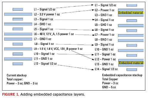
The
redesign is shown on the right-hand side of Figure 1. The top
FaradFlex® core is used for the 3.3 V supply, and the bottom one for
the 1.5 V supply. The thickness of the 1.5 V/Ground plane pair in the
center of the stack up remains approximately the same.
Three
versions of the new 14-layer PCBs were manufactured, in addition to the
standard 12-layer board. The new 14-layer PCBs were manufactured using
BC24, BC12, and BC12TM materials as the thin laminate cores,
respectively. These boards are denoted as BC24, BC12, and BC12TM in the
descriptions and figures that follow. The standard 12-layer boards are
denoted as FR-4 for simplicity.
BC24 and BC12 are
modified epoxy substrates that are 24 and 12 micrometers in thickness
respectively. BC12TM is also a 12 micrometer material but has high Dk
ceramic particles added to raise the Dk to 10 from the 4.4 of the
unfilled products. The materials are formulated to insure durability
during PCB processing. The copper foil is a special low profile version
to minimize the chance of shorts or leakage. The material is
manufactured and distributed under the Buried CapacitanceTM license of
Sanmina-SCI Corporation.
To evaluate the
performance of the FaradFlex materials, the BC24, BC12, and BC12TM
boards were populated only with bulk decoupling capacitors, and the
FR-4 board was fully populated with bulk and high-frequency SMT
decoupling capacitors. Compared to the standard FR-4 boards, the
embedded capacitance boards had 781 SMT capacitors removed. The
decision to remove all the decoupling capacitors was based on the
results of the simulations and that this methodology had proven
effective in previous designs.
The testing included
swept-frequency S- and Z-parameter measurements for both the bare and
populated boards, power bus noise measurements in both frequency and
time domains, pre-EMI scan, and environment chamber testing.
Good
correlation of simulated to measured performance was recorded. Thin
capacitor substrates do have an effect on the characteristics of
power/ground planar power bus structures. In general, the voltages are
more stable with greatly reduced resonances. By using thin core planes
and simulation tools the number of discrete capacitors can be reduced,
and electrical performance is improved. Besides reducing the number of
discrete capacitors used, there is also a reduction in power/ground
plane resonance that minimizes the amount of electro-magnetic radiation
from the board.
Product Build
The
newly designed 14-layer embedded capacitance PCBs were manufactured
using ZBC™ layer processing. Minor wet process allocations were made to
process the thin cores along with a recommended 500-volt HiPot test for
the cores prior to lamination and a final PCB 500-volt HiPot after
test. All manufacturers that currently process 0.002 inch core
materials should be able to process these materials with minor
process/handling changes.
Performance/DC Capacitance of Bare Boards
The
DC capacitance of the 1.5V/Ground pair, as well as the 3.3V/Ground
pair, was measured for all four types of the bare boards. Two methods
were used, and the results were either directly obtained from an LCR
meter or indirectly derived from vector network analyzer measurements.
As shown in Table 1, the results from the two methods
agree within less than 10% (results from the network analyzer are in
parentheses in the table).
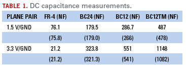
The
capacitance cores significantly increased the DC capacitance values
(from between 60-80% for the 1.5V/GND plane pair and from 93-95% for
the 3.3V/GND plane pair). The BC12TM cores achieved the largest
capacitance values as expected. A large DC capacitance is beneficial
for power bus as it can store more charge for logic transitions, as
well as decrease power bus impedance at low frequencies.
An
interesting observation is that the DC capacitance values are larger
for the 3.3 V/Ground pair than the 1.5V/Ground pair in the embedded
capacitance boards. That is because the bottom 1.5 V plane shown in is
a split plane, and the area of the 1.5 V is only approximately one
third of the total board area. Therefore, the increase in DC
capacitance is less significant due to the reduced plane area.
Product Performance/Swept-Frequency Measurements of Bare Boards
The
swept-frequency parameters are good indications of the impedance of the
power/ground plane pair. Specifically, |Z11| is the impedance of the
power bus (power/ground plane pair) looking into a port. It determines
the noise voltage generated in the power bus due to a current drawn at
the same port. However, |Z11| measurements can be dominated by the port
inductance at high frequencies. In such cases, transfer impedance,
|Z21|, can reveal information that is otherwise buried in the input
impedance results. The scattering parameter, |S21|, between two
different ports in the power bus, which is a function of the transfer
impedance, |Z21|, is often used to study the noise voltage generated in
the power bus due to a current drawn from another location away from
the observation port. For both |Z11| and |S21|, a lower magnitude
indicates a lower noise voltage generated in the power bus due to the
same amount of noise current. In other words, the lower the magnitude
is, the better the power bus performance.
Bonding
pads designed for decoupling capacitors were chosen as the testing
ports, and the S-parameters were obtained from a vector network
analyzer.
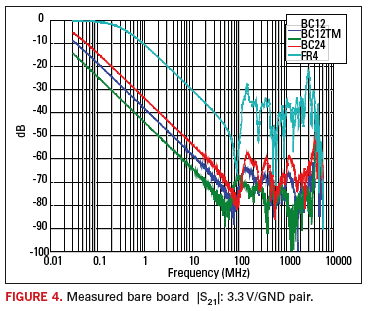
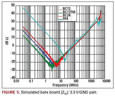
Figure 2 and Figure 4 show the |S21| versus frequency curves for the 1.5 V/GND and 3.3 V/GND pair, respectively, while Figure 3 and Figure 5 show the corresponding |Z21| results that are calculated from the S-parameter measurements.
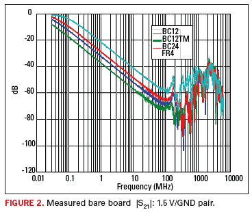
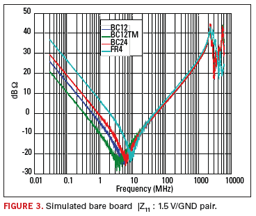
At
frequencies below 10 MHz, all the curves clearly demonstrate that the
BC12TM boards have the lowest power bus impedance; hence, their
performance in noise reduction in this frequency range is the best
among all types of the boards. BC12 is slightly trailing behind,
followed by BC24. The standard boards are obviously the worst.
Product Performance/Time-Domain Power Bus Noise Measurements
Time-domain
power bus noise measurements were taken when the boards are running
under a pseudo-functioning script. Again, bonding pads for decoupling
capacitors were used as ports, and a flexible coaxial cable was used to
connect the port to the Agilent Infiniium 54855A Digital Sampling
Oscilloscope. The AC noise voltage was measured using a DC blocking
capacitor to prevent damage to the oscilloscope.
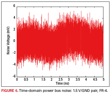
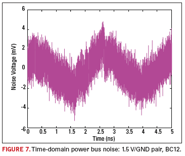
Figure 6 shows the power bus noise voltage in the 1.5V/Ground pair measured at one location on the FR-4 sample. Figure 7
shows the measurements for the BC12 boards. Similar time-domain
performance was noted for the other capacitance materials. All of the
materials produced a PCB with less noise than the standard FR-4 board.
For the 1.5 V/GND pair, the peak-to-peak noise voltages are
approximately the same for all types of the boards and dominated by the
lower frequency envelope. The higher frequency noise for the 3.0 V/GRD
pair is likewise reduced and the overall peak-to-peak noise voltage was
lower than the FR-4 board.
The
embedded capacitance boards resulted in lower power bus noise. This was
achieved when all the high-frequency SMT decoupling capacitors were
removed. The redesigned boards functioned correctly with only the
embedded capacitance layers and bulk decoupling capacitors.
Product Performance/Frequency-Domain Power Bus Noise Measurements
The
power bus noise at the same port locations was measured in the
frequency domain as well. An Agilent E7404A EMC Analyzer (a spectrum
analyzer) was used with a resolution bandwidth of 10 KHz. Again the DC
component was filtered away by a built-in DC block.
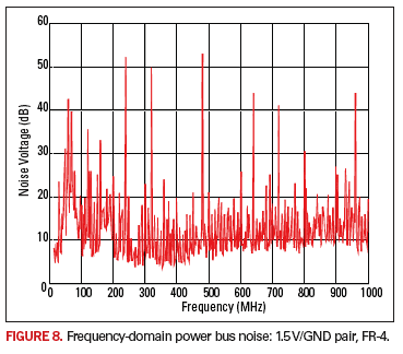
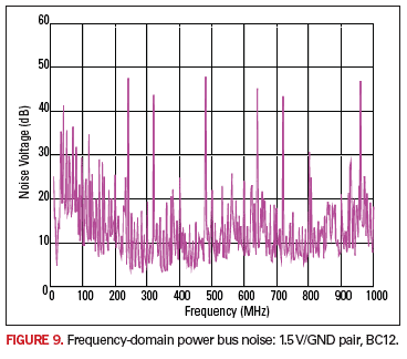
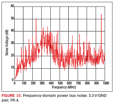
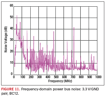
The results in the 1.5 V/GND pair in the frequency band from 10 MHz to 1 GHz are shown in Figure 8 and Figure 9, the FR-4 and BC12 boards, respectively. The corresponding 3.3 V/GND pair results are presented in Figure 10 and Figure 11 for the same boards.
It
is quite difficult to draw definite conclusions from these
frequency-domain results due to their complexity. Although the noise
voltages at some frequencies are lower in the embedded capacitance
boards (for example, at the three peaks between 200 MHz and 500 MHz as
shown in Figure 8 and Figure 9), the noise magnitudes at some other
frequencies are actually higher. Measurements at frequencies higher
than 1 GHz may assist in the development of insight.
Simulation Results
Simulation
was performed to compare the result with actual board measurement
utilizing EMIStream developed by NEC. This simulation calculates
impedance |Z11| of a power plane based on PEEC (Partial Element
Equivalent Circuit Model) method and Spice simulation. The parameters
for this target PCB such as thickness between power and ground plane,
Dk and copper thickness have been set prior to running simulation. Also
the excitation point has been set at the exact same point as where the
actual board measurement was probed.
The simulation results for 3.3V/GND plane shown in Figure 12
compare the results of standard FR-4 boards to the BC24, BC12 and
BC12TM boards. As shown in Figure 5, at the low frequencies below 20
MHz, BC12TM board had the lowest impedance followed by BC12 and BC24.
Standard FR-4 had the highest impedance.
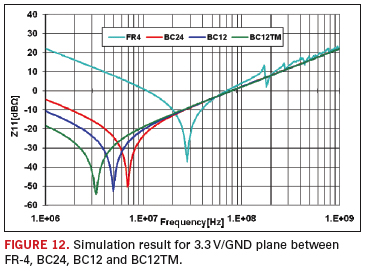
Apparently,
the simulation results shown in Figure 12 and the measurement results
shown in Figure 5 are well correlated. This proves the possibility of
calculating impedance with PCB information before fabricating a board
for optimum PDN design.
Cost/Performance Analysis
The
cost of a embedded capacitance printed circuit board assembly is
compared against a standard material assembly for this application.
Taking into consideration the cost reduction by removing the capacitors
and their associated assembly cost, the estimated cost increase is 8%,
15%, and 26% for the BC24, BC12, and BC12TM assemblies respectively.
One reason the cost was higher is the fact that the board had to be
redesigned from a 12-layer to a 14-layer product. For many applications
the layer count would remain the same. Also, the BC materials are more
expensive than standard FR-4 materials.
One of the
most significant advantages for embedding the capacitors is the area
that is freed up for routing traces, and the potential to decrease the
size of the board. Depending on the application, mechanical constraints
and the number of capacitors required, these benefits could contribute
to overall improvements and faster time to market. The cost differences
and benefits will vary depending upon the application and volume.
Conclusions
Initial
measurements and simulations clearly demonstrate the benefits of these
embedded capacitance materials used in the power/ground plane pair, in
terms of lowering power bus impedance and reducing power bus noise.
These thin power/ground layers achieved a comparable or even better
performance with bulk decoupling capacitors only.
The
simulated and actual results compared favorably, and the decision to
remove all the decoupling capacitors proved to be effective. Although
the initial cost analysis of implementing buried capacitance is higher
than the standard board with capacitors, there are other benefits to
complete the analysis. Designs that do not need additional layers to
achieve the embedded capacitance, as an example, will be easier to cost
justify. PCD&F
Ed note:
This article is a synopsis of the simulated and measured product data
related to the performance of buried capacitance layers. Additional
details can be found in the paper entitled “Utilization of Buried
Capacitance – A Case Study” presented at DesignCon 2008.
Acknowledgments
We would like to acknowledge our respective companies and UMR for supporting this study.
Jun Fan is a professor at the University of Missouri-Rolla; This email address is being protected from spambots. You need JavaScript enabled to view it.. Norm Smith is a design engineer and Jim Knighten is an EMI and signal integrity engineer at Teradata; This email address is being protected from spambots. You need JavaScript enabled to view it., This email address is being protected from spambots. You need JavaScript enabled to view it.. John Andresakis is vice president of strategic technology at Oak-Mitsui Technologies; This email address is being protected from spambots. You need JavaScript enabled to view it.. Yoshi Fukawa is president of TechDream; This email address is being protected from spambots. You need JavaScript enabled to view it.. Mark Harvey is an engineer at Sanmina-SCI; This email address is being protected from spambots. You need JavaScript enabled to view it..


