FPGA/PCB Co-Design Increases Fabrication Yields
When integrating FPGAs into PCB design every signal and pin has a measureable effect on production yield.
PCB designs with field-programmable gate arrays (FPGAs) are often
done more empirically than systematically – the board is designed and
then “tweaked” by altering component placement, component orientation,
PCB layer stack up, PBC signal layer pairs, trace routing, and even
manufacturing materials.
As FPGAs have become a more
dominant design component, the concept that the FPGA pinout can be
optimized for both internal and external FPGA signal integrity (in PCB
design) provides a flexibility not available with competing
technologies. Taking advantage of that flexibility throughout the
design process can measurably increase PCB yields and increase profit.
Incorporating FPGA/PCB co-design and paying special attention to FPGA
placement and routing can reduce “tweaking” time by 20-50%, increase
fabrication yields, and ultimately increase the end-product’s
profitability.
FPGA Devices Dominate New Designs
A
decade ago, ASICs were the dominant definable component found in design
starts. Today the flexibility, rapid deployment, and lower development
costs of FPGAs have resulted in the dramatic increase of their use in
new designs.
As FPGAs have matured as circuit
elements, pin count has risen significantly. The increase in pin count
represents a factorial-increased complexity to the PCB design. This
complexity increases with greater numbers of traces, vias and tighter
tolerances, plus signal integrity and timing constraint issues. The
increased pin count also creates the need for additional layers as
well, each adding 10-20% to the manufacturing cost of a completed board.
Typical Design Flow
Having
evolved from different technology arenas, PCB and FPGA designs have
some differences in design flows that have hindered many co-design
efforts and negatively impacted the optimization of the FPGA-PCB
interface. PCB designs use a schematic-based data entry method. FPGAs,
however, are defined by a language-based description. This difference
in methodologies coupled with human interface issues has been at the
root of most problems.
In a typical design, the
FPGA team defines high-level block diagrams comprising the system
design. At this point, the logical function of the device has been
defined, generally as VHDL or Verilog code, but very little effort has
been put into defining the physical connection of the FPGA.
Next,
the FPGA team concerns itself with the most critical signals.
Typically, these are all the high-speed signals, including the clocks.
These signals are defined and locked during the FPGA synthesis step.
The
FPGA vendor will then use place-and-route software to assign the
remaining logical signals to physical pins, creating a pin map file,
which almost always requires several iterations before the pinout is
both physically and mechanically optimized.
Only
then does the PCB design team become involved. Once the pin mapping is
complete, the data is transferred to the PCB team, where it is defined
by the librarian for use in the PCB design. This transfer by the
librarian is almost always done manually and therefore is also a source
of possible error.
Finally, the PCB designer
instantiates the FPGA symbol into the PCB schematic, and it then goes
to PCB place and route. Because the PCB design has not been a factor in
the system design until now, the need to add extra board layers because
of complex pin maps are not uncommon.
From here, the
design enters the “tweaking” phase mentioned earlier. In this process,
the flexibility of the FPGA pinout is often used to optimize the signal
integrity and timing of the PCB.
In many designs,
the need for tweaking has been exacerbated by the good intentions of
the FPGA design team. In an effort to involve the PCB design team, the
FPGA locks in the I/O pin assignments early in the process, but later
finds that the pin assignments result in PCB layouts that can’t meet
signal and timing specifications, or that they must change pinouts for
other reasons. The result is that the FPGA pinouts must be reconfigured
and the PCB re-spun.
While it’s clear that the
flexibility of the FPGA is a great help in solving many PCB signal and
timing issues, this flexibility is not typically used far enough ahead
in the process to prevent the issues that require tweaking later in the
design process.
Increasing PCB Yields
Two
ways to increase PCB yields are well known. Decrease the number of
layers, and complete the design of the board with as few iterations as
possible, and fabrication yields increase. Other techniques, such as
shortening traces and minimizing the number and length of vias, can
also increase yields. Longer traces not only require more board space
but also increase the risk of crosstalk, noise, and signal coupling
that can compromise timing. Vias can become problems due to mechanical
stresses and vibration.
Certainly, PCB design teams
consistently employ the techniques mentioned above, as well as others,
to increase the manufacturing yield of PCBs. However, the later the PCB
design team enters the FPGA design process, the fewer the number of
successful and contributory options there are available. In the worst
case, a routable board may not be achievable, or the only viable
solution may be to add layers, thereby reducing yields as well as
increasing the cost of the PCB.
What is needed is to
involve the PCB team earlier in the FPGA design, using a tool that can
understand both a PCB schematic representation and the FPGA design
language. Further, the tool must be able to quickly translate design
changes between both domains.
Concurrent Software I/O Designer
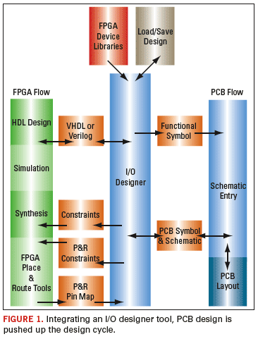
Figure 1
graphically illustrates both the FPGA and PCB design flows.
Essentially, this is what has been previously described as a
“traditional” design flow. In Figure 1, the center bar represents the
co-design software I/O design management tool function previously
discussed. This I/O design tool would dynamically manage communications
between the two design flows, providing data when required, keeping
both design flows up-to-date, and allowing the flexibility of the FPGA
to be maximized.

Contrasting
Figure 1 with the earlier design description, it can be readily seen
that the PCB team involvement has been moved to much earlier in the
overall design process – all the way back to the initial VHDL/Verilog
description. Using an available software tool like this one, the I/O
design manager can monitor the FPGA flow and update the PCB with the
current data.
Beginning with the intial
language-based description schematic derived earlier in the process,
from the initial language-based description, the schematic is revised
as each definition from the FPGA is learned. This early schematic may
have all the pins assigned, or only the critical pins. As electrical
and physical constraints are defined, their influence is accounted for
in the PCB design, and as pins are assigned in the FPGA flow, they
become defined on the PCB design.
The benefits of
automation in the PCB pin definition process should also not be
overlooked. Any manual transcription of data introduces the chance of
error. The greater the number of transcription operations, the greater
the chance and likelihood of resultant errors.
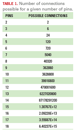
Looking at the values listed in Table 1,
you can see that each signal (S) has S! (S factorial) number of
interface connections. Thus, a two-pin package has two interface
connections; a four-pin package has 24, and a 100-pin FPGA has 9 x
10157 connection combinations. Microsoft Excel cannot even calculate
the connection possibilities for a common 1000-pin device (see Table
1). Clearly, the potential for error when manually transferring pin-map
data is extremely high.

Also, the
tools are not one-way data transfers, and constraints can be defined on
the PCB side that reflect to the FPGA side. And of course, the real
beauty of the FPGA is that its design can be altered to optimize
external connections.
By allowing the PCB design flow
to feed back data to the FPGA design process, all aspects of the PCB
design can be optimized. Trace lengths are minimized, and the number of
layers and therefore the number and length of vias are reduced as well.
The Bottom Line
Without
question, increased pin count and decreased pin pitch on FPGAs will
continue. As this trend marches forward, design complexity will dictate
that the best way to increase PCB yields in the shortest possible
design time is through the cooperative and parallel design of the FPGA
and the PCB.
Software tools are now available that
provide the I/O designer with the tools needed to perform this precise
function. As with high pin counts, several variables can contribute to
reduce yield, increase design time and negatively affect profit margin.
Among these are long design times caused by pin map entry errors and
resulting PCB reiteration, longer-than-necessary traces that affect
timing and signal integrity, and unnecessary PCB layers and vias that
increase manufacturing cost and reduce reliability.
In a PCB design integrating an FPGA, quite literally, every signal and pin has a direct and measurable affect on production yield and profit. Incorporating software that helps manage and mitigate the co-design of the FPGA and PCB is imperative to realizing maximum yield potential. PCD&F
Yan Killy is a technical marketing engineer for Mentor Graphics’ system design division; This email address is being protected from spambots. You need JavaScript enabled to view it..


