EMI/EMC and SI Effects from Ground-Return Vias on PCBs
At higher frequencies signal loss and noise is reduced when ground-return vias are placed close to the signal vias.
There is often a lively discussion when it comes to the importance
of “ground” or ground-return vias for high-speed signals that travel
from layer to layer in a PCB. Many claim that there are many ground
vias that stitch together the various ground layers, so there is little
concern about their exact location. Others will insist that the
ground-return vias are important to both EMI/EMC and SI performance for
high-speed signals. The real truth lies somewhere in the middle. It
depends on the data rate of the signals, and the amount of signal loss
and/or noise generated between the planes.
The basic
issue is that when a signal travels from one reference plane to
another, it may travel through a pair or more of board layers. The
return current must also travel from one plane to another. If a nearby
metal conductor (ground-return via) is provided, the current will
spread out between the planes, using the natural displacement current
of the capacitance between the planes. The distance the current will
spread is determined by the board’s operating frequency, its dielectric
thickness, and the amount of inductance associate with the return
current path.
Current will always take the path of
least impedance. This means the distance the current will spread
depends on the impedance caused by the loop inductance of the path
created by the signal via and the current return path. This spreading
distance becomes very small at high frequencies (> 1 GHz) and any
benefit from a ground-return via will only be realized if the ground
return via is close to the original signal via.
Single Plane Pair Transition
We
can start by examining the signal loss seen by a high speed signal
traveling through a single plane pair, changing reference planes from
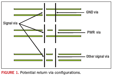
one plane to the other. Figure 1 shows several
configurations for the planes and potential ground-return vias. Figure
1a shows a signal via and a ground-return via connected to both ground
planes. Figure 1b shows the configuration if one plane is ground and
another plane is a power (or other) layer. Only one plane is connected
to the potential return via in this configuration. Figure 1c shows the
configuration when the potential return via is not connected to either
plane, or if a second signal via is nearby the original signal via.
First,
if we examine the loss for the signal, using S21 as a transfer function
of signal “in” versus signal “out”, and we move a ground-return via
(Figure 1a) to various distances from the signal via, we can see the
impact in Figure 2. Frequencies below approximately 1
GHz are not impacted by the location of the ground-return via. However,
higher frequencies have significant impact on the amount of loss to the
signal. If we are using a 2 Gb/s signal, the first harmonic is at 1
GHz, the third harmonic at 3 GHz, etc. Figure 2 shows that the first
and third harmonics are not greatly impacted by this return via.
However, if a 6 Gb/s signal is used, the first and third harmonics are
at 3 GHz and 9 GHz, respectively. Placing a ground-return via only 50
mils from the signal via can improve the 3rd harmonic by more than 1
dB, which can be very significant, especially for long trace lengths
where losses, including dielectric loss, can have a major impact to the
signal quality.
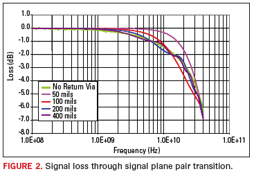
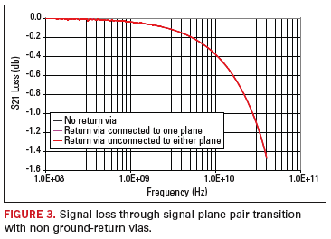
Figure 3
shows the impact of removing the ground-return via while keeping the
return via configurations in Figures 1b and 1c. There is no discernable
difference between these return vias and having no ground-return via.
Clearly, other signal vias and power vias cannot be assumed to provide
a return current path for the original signal via.
Multiple Plane Transitions
Now,
lets consider a PCB where there are multiple layers – for example, a
backplane PCB. We can perform the simulation again for any number of
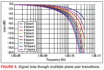
plane pair transitions. Figure 4 shows the signal
loss as additional plane pair transitions are added. Three planes mean
a 2-plane pair transition, and so on. As additional planes are added,
the signal loss increases, especially at high frequencies.
When
a ground-return via is placed in close proximity to the signal via, the
loss can be improved, even for a greater number of plane-pair
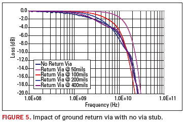
transitions. Figure 5 shows the impact of a
ground-return via when the transition is all the way through a many
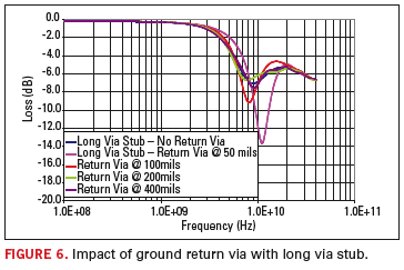
layered PCB with no via stub. When a large via stub is present, and the
signal simply transitions from one layer to the next, the results in Figure 6 show that a ground-return via can again help reduce signal loss.
EMI Effects
Another
way for via transitions to impact EMI is for noise signals to be
launched between planes and coupled onto other vias or connector pins
some distance away. Again, the location of a ground-return via can
significantly improve (reduce) the amount of this noise launched
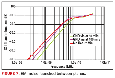
between planes. Figure 7 shows that the impact is
greatest between 1 to 10 GHz, and above about 10 GHz the difference was
minimal. Using the previous example, at 3 GHz, a ground-return via
placed 50 mils from the signal via would reduce the noise injected
between the planes by 6 to 7 dB, easily making a pass/fail difference
in some systems.
Summary
The
question of whether a ground return via needs to be placed close to a
signal via can be resolved only when the frequencies of interest are
known. At lower frequencies, these ground-return vias are not critical,
and normal ground-to-ground stitching can be used to provide a suitable
return path. However, at higher frequencies, the amount of loss to the
intentional signal’s harmonics and the amount of noise injected between
the planes (and potentially escaping the system metal enclosure) can be
significantly reduced when a ground-return via is placed close to the
original signal vias. Return vias that are not connected to both planes
will not provide the needed improvement. PCD&F
References
1.
Xin Chang, Bruce Archambeault, Matteo Cocchini, Francesco De Paulis,
Vysakh Sivarajan, Yaojiang Zhang, Jun Fan, Samuel Connor, Antonio
Orlandi, and Jim Drewniak. "Return via Connections for Extending Signal
Link Path Bandwidth of Via Transitions,” accepted for publication in
EMC Europe Symposium, September 2008.
Dr. Bruce Archambeault is an IBM Distinguished Engineer and IEEE Fellow; This email address is being protected from spambots. You need JavaScript enabled to view it..


