Optoelectronics Comes of Age
Optical interconnects are expected to significantly increase computing power in products with ultra-high frequency data rates, increasing its usage over the next 5 years.
Optical interconnections are being considered for use throughout the backplane, in the motherboard, to or from adjoining daughter cards or from any number of associated interposer peripheral boards. Several years back, people were talking about “optical interconnect” and “embedded waveguides” especially in the high-speed industry. Then, improvements in high frequency copper signal transmission changed the market, and the discussion of “opto” declined to almost nothing.
Today, implementation of optical interconnection technology is reappearing as a method to resolve or reduce the impact of issues associated with increasingly high frequency data rates beyond 10 GHz and aggregate data rates in the terabit/sec realm. The use of optoelectronics in these applications is expected to significantly increase overall computing power.
There are some concerns about the use of copper, particularly for 10 to 20 Gbps or higher products, where EMI can be a problem. This is particularly true in aerospace and military environments. Also, as package density increases, heat dissipation capabilities are reduced, and the costs associated with a copper solution increases exponentially. Even with these high-speed requirements looming large on the horizon, it is anticipated that the widespread commercial implementation of optoelectronic solutions remains at least five years away. For most applications, whether it be telecommunications, computers or data transmissions, there are a broad range of optical capabilities that must become available to facilitate a complete optical interconnection system. The optical capability also needs to be compatible with the complete electronic system to permit the creation of hybrid configurations.
Application-driven capabilities, such as on-substrate based waveguides, are optical signal carrying “wires.” They are typically glass fibers that can be incorporated in films and placed either on the surface or embedded, off-substrate such as with a flexible and/or bendable link. The system will also include coupling interfaces and connectivity to light sources and photodetectors. In addition, application specific compatibility and reliability must be met for reasonable manufacturing assembly processes, thermal mechanical environmental impact, and lifetime requirements. Substrate connectivity starts from the backplane or motherboard and continues through to the chip level, typically on or in association with the daughter boards.
The signal must also move between chips on multiple boards and ultimately back out off the motherboard. These same optical capabilities are also applicable to stand alone packaged transmitter and receiver applications and for substrate-based or stand alone functional splitters, star couplers or other components providing functionality. The point here being that requirements and capabilities meeting practical substrate based applications are also essential for a broad range of diverse optical interconnectivity solutions.
This article reviews the generic capabilities for a practical optoelectronic substrate interconnection system, the substrate associated polymer waveguide capabilities and requirements, and evolving practical embodiments under development today.
Historical Comments
Test installation on manufactured low loss optical glass fibers for telecom applications first began in the late 1970s. By 1985, a multimode optical fiber link used by Bell Atlantic (now Verizon) between Washington and New York was proudly demonstrated to one of the authors. Shortly thereafter, single mode glass optical fiber was manufactured for installation, and as quality improved over the next decade, glass optical fiber became practical for central office and undersea installations. The rest is history, as optical fiber now brings phone, TV, and internet to the home as well as spanning oceans for telecommunications.
During the mid 1980s as optical fibers moved onto PCBs and into computers, it was recognized that short interconnecting links and optical function components, such as splitters, combiners, etc., would be needed at low cost.. Many fiber technology approaches were developed and commercialized to provide the required functionality. In addition, laboratories worldwide invested considerable effort in the development of planar sheets of polymer waveguides.
Optical Signal Distribution Requirements
A broad range of optical capabilities must be utilized to facilitate a complete optical interconnection system. Optical fibers and polymer waveguides are providing practical hybrid solutions that are beginning to meet industry requirements. Both point-to-point optical links and functionality for signal distribution options combined with appropriate connectivity solutions are being explored, prototyped, and implemented. Subsets of these capabilities are being utilized for stand-alone off-substrate functional components. Optical InterLinks polymer waveguide technology exemplifies how the critical attributes can and are currently being met for specific application developments and will be used as examples of evolving practical systems. Capabilities for a complete optical interconnection system involve the following categories.
1. Optical input and output connections at the edges of the motherboard or backplane. For some time optical fibers at the board edge have been used to connect directly to photo detectors and laser sources. Single fiber, multiple fibers in ribbons, or cables are used for these board inputs. Solving problems caused by copper transmission lines on the board, such as high signal input/output density, EMI, high energy consumption and associated heat dissipation, plus physical constraints such as the forces required to couple high-pin-count/high-density connectors, are increasingly driving the use of optical transmission into the motherboard and on through to the daughter boards.
2. Backplane/motherboard (BP/MB) optical signal distribution. Board edge connector coupled optical signals are distributed across the backplane to the daughter board assuming there are no active components on the BP/MB. Depending on the board size and the length of the optical runs required, either fibers/fiber ribbons or polymer waveguides can be used. Since optical fibers have lower optical loss, they are preferred for long runs typically covering from 30 to 100 cm. Fibers will likely be in the form of bundles or ribbons, and are frequently encapsulated into commercially-available polyimide sheets pre-arranged in a flexible film package. Fiber shuffles for signal distribution can be mounted on the BP/MB to uniformly route optical I/O between all daughter boards as required.
Parallel polymer waveguide links can be used to distribute signals from short millimeter lengths (up to 50 cm runs) depending on optical loss at the operating wavelengths and the allowable system loss budget. In some board systems this is in the 10 to 15 dB (~5% signal remaining) range. It can also be advantageous to choose polymer waveguides that have unique functionality, like low-loss crossovers for routing, splitters, star couplers for mixing and distributing, and/or combiners, that can be incorporated in planar waveguide films.
Both fibers and polymer waveguides films can be attached or bonded to substrates, be embedded within or between boards, or be a flexible off-substrate circuit attached only where needed at the end connections. BP/MB optical signal distribution typically provides routing to right angle oriented daughter boards where active light sources, detectors and logic chips are located. Of course, for a single board system containing active components, fiber arrays connected to fiber or polymer guides at the board edge are used to directly interconnect components.
3. Right angle connectorization at the daughter board (DB) junction with the BP/MB. Right angle board-to-board connectivity is required to couple light between DBs and BP/MB that interconnect 90 degrees to each other. Low cost, high-performance, right angle array connectors are critical for this application, and considerable efforts in the industry have been made to achieve a practical solution compatible with electronic counterparts on the daughter board.
To achieve DB-to-DB connectivity along the BP/MB, waveguide arrays need to enter the BP/MB connector housing from both directions. To achieve dual-directionality typically requires multiple waveguide array interconnects be stacked in at least two or more layers, in order to be able to direct signals from daughter card to daughter card along the BP/MB. The use of closely spaced waveguides enables very high-density interconnections within a standard MT (multi-terminal) form factor, or other custom two pin aligned ferrule options.
An MT connector is a commonly used fiber optic ribbon connector. With appropriate machining, it is modifiable to provide free standing board edge planar polymer waveguide array coupling alignment. The MT ferrule connector is very popular due to its small form factor and the ability to connect 24 channels with 12 channels on two rows (greater numbers, space permitting) while maintaining conventional optical fiber 250 microns pitch spacing. Machining modifications enable coupling of up to several hundred closely-spaced polymer waveguides for high-density interconnectivity. Typically, MT ferrules are inserted into flexible aligning and locking housings to provide a latchable connector tightly holding the coupling interfaces together with a zero air gap. These latchable housings are commercially sold under manufacturer’s names, such as MPX or MPO connectors.
For right angle board-to-board optical interconnections, when the daughter card is inserted, the locking mechanism assures a zero air gap interconnect between adjoining ferrules, allowing sufficient insertion force flex to be compatible with adjoining electronic pin connectors on the daughter board. This configuration assures good coupling while avoiding a hard stop insertion of the board. Thus the natural bend flex of self-supporting waveguide films is important. On the other hand, unique lens configurations are also being explored to provide practical coupling solutions allowing a more forgiving air gap. Both are useful for high vibration environments.
Both electronic and optical connector housings should have nearly identical height and at least compatible form factors at the edge of the DB and on the BP/MB. For these applications, spring-loaded latchable housings with internal custom ferrules are the preferred choice for optical configuration. Once the optical signals are on the DB, polymer waveguides offer unique versatility where array routing and optical functionality is required to distribute signals through the daughter card.
4. Optical signal distribution on the DB or into Tx/Rx link packages. Optical signals on DBs are distributed directly to components or to small interposer boards for subsequent distribution to and from typically VCSELs (vertical cavity surface emitting lasers) and detector components. Traversing the offset space between the parallel DB and the interposer board requires either flex optical waveguides and edge connectors, or lens and I/O mirror arrays to couple the DB and small board offset air gap. Waveguide array transmitted signals are coupled directly to detectors (PD) or from the VCSELs, with both components close to their amplifiers or driver chips. Increasingly the capability and versatility inherent in polymer waveguides is a prime consideration for DB signal distribution. Some of the enabling capabilities and attributes for polymer waveguides include:
- Point-to-point dense arrays as flexible links (unattached except at the terminations) or substrate-attached links or combinations.
- The ability to provide complex routing under, over or around surface mounted components or with waveguides embedded between board substrates to be routed from the underside of the board to the surface component side.
- Functionality, including splitters, combiners, star couplers and crossovers to redirect the normally parallel arrays.
- Coupling with I/O mirrors for out-of-plane component interfaces from above or below, as has been demonstrated with top-surface or flip-chip interfaces respectively.
5. Other optical interconnection systems. Combinations of 1 through 4 taken separately can be used for a number of polymer waveguide optical interconnection applications. These include separately packaged optically interfaced transmitters, stand-alone functional components, optical sensor read heads, and biosensors. In addition, custom or conventional ferrule-based connection options are allowing interface fiber shuffles and fiber distribution harnesses to connect to boards or components.
Board Level Polymer Waveguide Creation
Versatile and practical interconnection solutions are achievable with optical polymer waveguide technologies that incorporate the distribution requirements summarized previously. In particular, practical cost-effective optical interconnections can and are being created using generic procedures including the applications noted below.
- Waveguide design layouts for parallel links and/or functionality are created using waveguide design software such as R-Soft. These designs are then reduced to instructions to write high quality photolithographic masks.
- Polymer material and related constituent synthesis, purification, mixing/dissolution, filtration, coating, solvent removal and any materials preparation required for raw materials and film preparation. This provides material with the lowest optical loss to expose/process waveguides.
- Using appropriate process technology, waveguides are created with protective layers in self-supporting film sheets. We believe this is the preferred practical route to produce useful interconnects, as opposed to creating the waveguides on substrates for final application.
- Precise micromachining of the film sheets, typically by using excimer laser-based high-precision computer workstation micromachining with sub-micron resolution. The laser is used to separate the large number of imaged parts after exposure, and to precisely and reproducibly locate the waveguide array links and functional devices within each film structure. This would allow connectors and optical interfaces to be configured in large numbers. Out-of-plane reflective mirrors can also be created and metallized as needed.
- After all of the connections and interfaces are assembled, the links or devices are fully evaluated to assure high-quality performance before installation on the final substrates or in the package. Constructing prefabricated, self-supporting guides reduces the potential for high-value yield losses. If waveguides are alternatively created directly on the high value substrate, a defective waveguide would necessitate rework and/or the possibility of scrapping an entire high-value board.
- Final assembly of the optical and electronic components and full quality verification.
This generic procedural sequence to waveguide creation provides a useful understanding of a practical and cost effective route for the development and implementation of polymer optical interconnections for optoelectronic substrate connectivity.
Practical Application Configurations
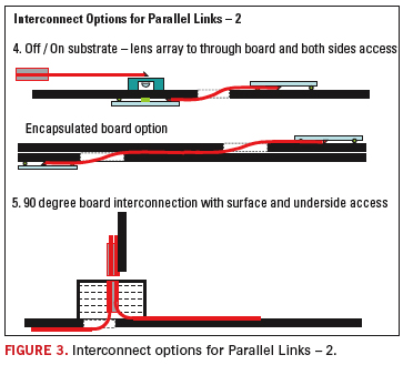
Waveguide interconnections can be designed and installed to be compatible with board interconnectivity for backplane/motherboard routing and coupling to either daughter boards or single boards. Interconnectivity to the sources and detectors associated with electronic chips is facilitated by versatile optical configurations. A flexible yet strong encapsulating film (as shown in Figure 1) provides a thermomechanically-stable self-supporting structure. Versatile designs and flexible films permitting a variety of parallel optical link interconnect options are shown in Figure 2 and 3 and described below:

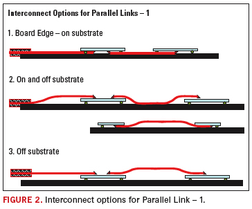
1. Substrate-surface-attached waveguides for board edge-to-chip interfaces or chip-to-chip coupling. Coupling to or from the chip is typically accomplished through flip-chip solder bump procedures using out-of-plane I/O mirrors. Solder bumps/balls are used for chip alignment and attaching components to the substrate.
2. Combinations that include on-substrate surfaces as in 1) above and a design that goes off-surface using flexible jumper style links to connect to the chip top surface. This configuration allows diverse connections such as board edge-to-chip, chip-to-chip or chip-to-off-board fiber-array ferrules.
3. Jumper style interconnectivity on both ends facilitating off-board or device package I/O leading to chip top access, and chip-to-chip options.
4. Hybrid options including either on- or off-substrate link to I/O mirror and lens arrays for interconnectivity to the underside of a substrate or to an optical layer in between substrates.
5. On-substrate or below-substrate surface waveguide arrays bending 90 degrees perpendicularly off board to connector ferrule and daughter board with edge connection ferrules. Using guide bending flexibility within motherboard ferrules enables daughter-board to motherboard connection compatibility with insertion requirements for connectors also on the daughter board. Lens coupling between the motherboard and the daughter board ferrules is being explored to allow for air gap and alignment tolerance instead of direct zero air gap contact coupling. Multiple stacked-waveguide film layers at the ferrule interface allow for array interconnections from daughter board to daughter board.
These interconnection options include a several critical optical interfaces used for: a) waveguides to/from optical fibers or b) waveguides to/from waveguides or c) waveguides from VCSEL’s, edge-emitting diode lasers, and to photo detector connections. These three basic optical interfaces are listed in 1 through 3 below and show in Figure 2 and 3. The fourth interface below is a fundamental optical guiding interface important for waveguides to/from graded index fibers.
1. Out-of-plane I/O (input/output) mirrors that deflect signals perpendicular to the waveguide film surface usually formed at the edge of a waveguide array film. Deflecting mirrors, optimized for each waveguide, are constructed in the film sheet, not at an edge.
2. Butt coupling, where the interface is typically cut perpendicular to both the waveguide film and the waveguides in the film plane.
3. Waveguide tolen array coupling including either 1 or 2 from the two previous examples above but with sufficient lens coupling distance of approximately 100 microns.
4. Optimum coupling between standard graded-index optical fibers requires compatibility or the near match of the propagating and transmitting angles (referred to as NA or numerical aperture match). Also, the lowest-loss coupling to and from these fibers requires reduced guide size for waveguide to fiber in order to couple into the higher fiber core index region at the core center for transmitter Tx interfaces, and for receiver Rx interfaces, guide sizes equal to or larger than the fiber core size to efficiently collect all fiber-to-waveguide coupled light.. Obviously bi-directional coupling requires a compromise on guide dimensions to best optimize the systems performance.
To meet specific application requirements, optical functionality can be imaged or incorporated within the parallel link waveguide films with appropriate coupling interfaces and configurations described above. Useful functionality may include crossovers, splitters, couplers, and combiners.
General Description for Optical Waveguides
Operationally, waveguides are “wire like” regions of higher refractive index within a surrounding matrix of a lower refractive index. Light propagating within the waveguide remains trapped inside as long as the glancing angle at the edge of the waveguide is not so large that light can escape. This phenomenon can be compared to the refraction of light as it passes through water.
Glass fibers are used for optical transmission applications in both telecommunication and data communications have a higher refractive index core that traps propagating signals. If the size of the higher index waveguide core is about 6 microns and embedded in 125 microns of lower index glass, light in or near the core can only travel in one path, with slight angular deviations. Think of it as a single lane tunnel through a mountain, where a driver has no option except to travel on the single path. An optical waveguide designed in this way is called a single-mode (SM) waveguide. Single mode waveguides are used for high data rate telecom signals that travel over long distances. All signals exit at nearly the same time and they are not blurred in the process.
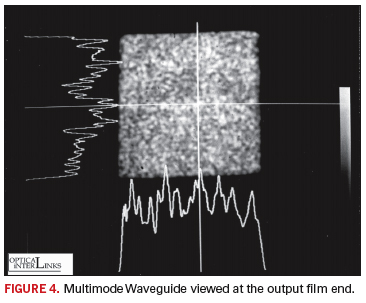
Larger core waveguides allow many signals to follow multiple paths. Again, using the analogy of a multi-lane highway tunnel, the driver can move back and forth taking either a straight or curving path through the tunnel. Thus, some “travelers” will get through the tunnel sooner than others. In optics, this type of waveguide is referred to as a multiple mode (MM) with specific angular values based on constructive and destructive interference of the nearly monochromatic laser light. A view of the output end of a 50 micron square multimode waveguide propagating many optical signals is shown in Figure 4. The granular light appearance is evidence of the many modes being propagated. Transmission times for these modes do not sufficiently blur the signal’s arrival, so MM waveguides are used for shorter (less than 100 meter) runs, even with very high frequency signals.
Other defining factors in optics require that the waveguide refractive index (or, the core to surround index) inside to be greater than the outside, in order to sustain higher propagating angles in the waveguide. If this index is too low the light escapes. Also, if the input angles are too great for a given index the light will also escape, analogous to porous tunnel walls.
Summarizing, SM waveguides are typically about 6 microns in width with a refractive index of approximately 0.006 over the surround sustaining propagation angles of within +/-7 degrees and are primarily used in telecom applications. MM waveguide cores range from 10 to 100 microns in width/diameter with a refractive index of approximately 0.02 to 0.035 over the surround and are primarily used for data communication links and circuit board interconnectivity. This high index difference sustains propagation angles of within +/-18 degrees inside the guiding core. For low-coupling loss, the interconnection offset precision for single mode waveguides requires +/-0.5 microns, while multimode guides of 40 microns widths requires within +/-5 microns offset precision. Thus, for substrate based optical interconnections, MM waveguides are preferred, given their higher tolerance for alignment offset and as such are less costly to manufacture.
Other important factors useful in optical interconnection includes smooth low optical absorption and low optical scattering waveguide walls, so that a sufficient percentage of the light gets through the link to solidly couple between sources and detectors.
Embedded Waveguides Between Substrates
Considerable discussion within the industry relative to creation and application of waveguide optical interconnections has revolved around attempting to embed optical layers within board substrates during the multi-layer board fabrication process. The idea is to align a polymer waveguide film sheet or link between two multilayer substrates (like FR-4 boards) then subject the board to the high temperature and pressure required to bond the substrate layers together in the board construction process. It is the authors’ perspective that this will cause problems in the construction of embedded polymer waveguides. Maintaining the less than 5 micron waveguide alignment offset tolerances required for multimode (MM) waveguides will be a challenge for any polymer system under a high temperature and pressure fabrication condition. These issues include (but are not limited to) thermally induced softening, pressure distortions as well as differential thermal expansion during heating and bonding. Even if a polymer waveguide system survived, creating the precise optical interfaces needed to connect components with waveguides trapped between two rigid millimeter thick (or possibly thicker) boards would seem to be an extremely complex difficult undertaking.
Some industry or university groups may have made progress in developing this technology, but that is beyond the scope of this article. Assuming that the technology advances to the point that embedded waveguide systems can survive the manufacturing process, maintaining waveguide array alignment and effective interconnection under these adverse pressure and temperature conditions is still and issue. Finally, manufacturing yield must be considered. There is still a question as to whether the potential manufacturing yield loss cost would be acceptable, since a process or material failure, or an alignment problem would likely necessitate scrapping of the entire board, which would be an expensive loss.
Alternatively, waveguide film sheets could be constructed and inserted with no prior machining for connecting two completed substrate boards, avoiding the high temperature and pressure construction process. Without pre-machining of the connection and optical interfaces, manufacturing difficulties for creating and metalizing in-situ mirrors at the base of open vias would be as much a challenge as insuring alignment under high temperature/pressure processing explained previously. To emphasize, alignment between surface components, vias, lenses, mirrors and waveguide structures must have less than 5 microns misalignment offset for acceptable interconnect system performance.
Over the last 20 years there have been many process and material technologies used to develop planar polymer waveguides containing films capable of meeting the current and evolving industry requirements. Sorting through the various techniques used to make polymer waveguides, these processes fall into two basic classes, both using photolithographic processes (sometimes with LDI) to define the waveguide. The distinctly different processes for the two classes are:
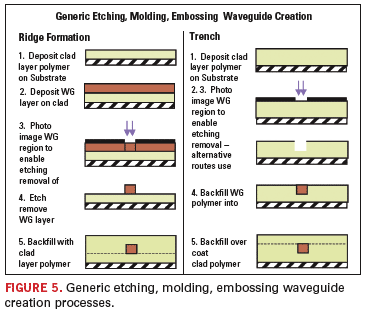
Ridge Technology. Initially, a polymer ridge or trench is constructed through molding, embossing, or etching that has a higher refractive index than the base polymer. See Figure 5 for a schematic outlining the generic process steps for ridge and trench polymer waveguide formation. The lower refractive index polymer surrounding the waveguide region creates the specific guiding properties. Different polymer materials have been evaluated depending on whether a ridge or trench is used to form these waveguides.
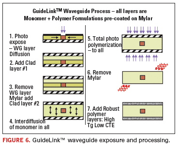
Diffusion Technology. This method includes the formation of a high refractive index waveguide by monomer diffusion into the light-exposed guide forming region with no mechanical or chemical etching contact. See Figure 6 for a schematic showing the diffusion technique process. An essential process feature here is the photomask-defined light exposure of a mobile monomer waveguide forming region in a polymer matrix that converts the monomer to a polymer. The process of continued monomer diffusion into the surrounding guide imaged region increases the density. The addition of other laminated monomer/polymer diffusing layers with the typical three-plus layer configuration is completely photo-polymerized after diffusion is complete. The essential steps include a light induced imaging reaction, a total polymerization light fixing for the entire film, and final cure, all using pre-coated dry materials without waveguide side wall contact. Light and molecular diffusion determine the guide walls.
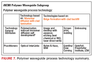
Several industrial groups and laboratories (some identified in Figure 7) exploring the ridge formation style technique also participated in an iNEMI study on optical backplanes. Over 15 groups participated to develop a polymer waveguide technology attribute table. Figure 7 shows the header for the resulting attribute table, listing the two polymer technique class types, with representatives from each subgroup. Both ridge and diffusion technologies have the capability to create self supporting waveguide films that can be micro-machined to provide fully connectable configurations ready for installation. The process techniques can also create waveguide films directly on the final application substrate. A number of unique performance and waveguide configurations can be obtained by the use of the diffusion or ridge guide forming processes.
Practical link configurations for optoelectronic substrate interconnectivity involves connectivity options for parallel and functional links. These critical system building blocks used for practical applications are described below, identifying and elaborating on key system attributes. Self-supporting waveguide films are used as the starting point. The basic features demonstrated confirm that practical connectivity is achievable.
Optical Interconnects and Connectivity Issues
In the following examples the coupling capabilities are demonstrated by the prototype products shown. Critical connectivity issues for practical applications of each are noted.
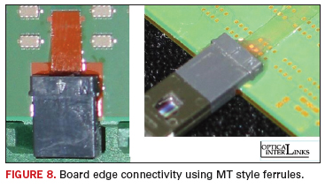
Type One uses substrate edge ferrules with similarly precise aligned waveguides and butt coupling interfaces. Butt coupling (surfaces cut perpendicular to waveguide or fiber axis) can be coupled to fiber arrays or to waveguide arrays held in similar ferrules. Figure 8 shows board edge MT ferrules connecting and aligning 12 waveguides to 12 optical fibers.
Critical connectivity issues include the need to prevent loss producing micro-bends at the connector interface where the film leaves the board edge into the modified MT ferrule. It is necessary to optimize performance to match fiber and waveguide allowed propagating angles (referred to as numerical aperture, or NA, defined as the sine of the half angle of the radiated Gaussian light pattern at the 5% intensity points) and waveguide dimensions, by matching fiber graded index profiles and waveguide step profiles. The connection needs to be matched with center-to-center spacing (pitch) to assure that maximum offsets are not exceeded. This is accomplished by using micro ferrules (machined slots for pin alignment required) designed for small array coupling footprints. In addition, it is necessary to couple to waveguide arrays on a high-density board with the several hundred interconnections using stacked waveguide films, and with a pitch less than the 250 micron limitation associated with standard optical fibers.
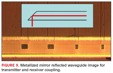
Type Two uses I/O mirrors cut at 45 degrees to deflect waveguided light perpendicularly from waveguide films to or from guides, sources or detectors components. An example of a waveguide deflecting metallized mirror is shown is Figure 9. Typically, unguided light path distances here are approximately 50 microns. The mirror surfaces are usually metallized to ensure that high angle multimode propagated light is reflected and not passed through a total internal reflection (TIR) mirror (without metallization). Propagating angles with reasonable mode fill are likely to exceed the total internal reflection critical angle allowed. Applications include substrate-attached guides for flip-chips or access to overlying components and top-access configurations used with flexible jumpers and functional devices not attached to the substrate. These mirrors can be cut at 45 degrees by microtome (thin blade used in tissue cutting) or excimer laser on the film edge. For mirrors in the center of waveguide film sheets, excimer laser micromachining will be used to create an “in-situ” mirror when required.
Precision alignment of the waveguide film arrays for reflected light coupling on substrates is critical, and is achieved first by precision cutting to locate the waveguides in the film strip. Figure 10 shows a 12-guide array precisely aligned to flip chip locating solder balls. Since alignment for each guide is critical (within +/- 3 microns for the example shown) runout or accumulated position error must also be within this range.
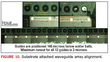
There are several conductivity issues with this type of waveguide. Alignment of the offsets with included runout over the entire waveguide array must match the part requirements before assembly. Runout/offset for vertical and horizontal waveguide positions relative to solder balls must be within tolerance for flip-chip component attachment. Care must be taken at assembly to prevent damage that can compromise waveguide and mirror performance. The waveguide film must fit with a uniform and minimum air gap under the flip-chip components. Alignment and waveguide performance must be maintained when subjected to IR solder reflow used for flip-chip attachment. Temperature stability of waveguide films the film’s optical properties must withstand prolonged exposure to temperatures up to 125°C.
In Type Three, the I/O mirror coupling to and from an array of lenses demonstrates the application for a flexible self-supporting waveguide link that bridges fiber ribbon arrays through a mirror with a lens through-board interconnection. An example is shown in Figure 11, with a side view schematic showing the installation configuration. With lenses, unguided distances can be increased to greater than 1 mm. Lenses facilitate imaging of component I/O with the waveguides through the mirror. This lens waveguide array requires several precise alignment shims to span this distance, in order to couple precisely with the waveguides. Applications can include traversing between top and bottom substrate surfaces or through boards connecting sources and detectors to the waveguide arrays.
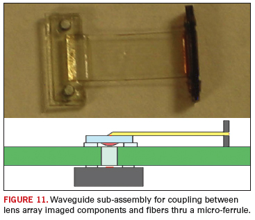
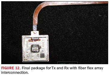
The critical connectivity issue with Type Three is that alignment for waveguides, lens elements and components must be within a few microns to ensure low loss connectivity. Optical fiber to waveguide array interface is achieved with an MT-like ferrule or micro ferrule for the example shown, using a flexible link not attached to the substrate that bridges to the outside of the package. Waveguide assembly, including fiber interface, mirrors, and the lens unit has a system loss of less than 1 dB (20%). The entire system loss is within operational specifications, including coupling from the four VCSELs through the system and back to four detectors. The final Stratos Optical Technologies TxRx unit (without cover) is shown in Figure 12. Alignment specs and tolerances for edge connections and mirrors are identical for this interconnect, including transmitter (Tx) and receiver (Rx) optimum-sized waveguides for high performance coupling to graded index fibers. Shown in Figure 13, the 60-micron guides are used for the receiver and the 30-micron guides for the transmitter.
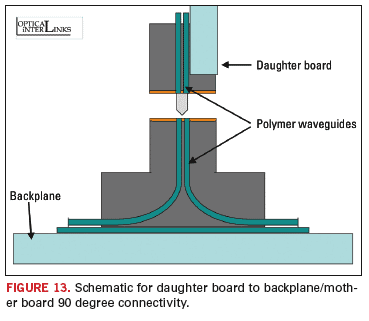
Type Four is based on board-to-board coupling for perpendicular connected substrates (as used for mother-to-daughter boards) which is achieved with ferrules in latchable housings, using butt coupling multilayer waveguide arrays.
The critical connectivity issues include the alignment and precision issues outlined in Type One (for MT ferule style connectivity). Particular emphasis should be placed on polymer waveguide-to-waveguide interconnection through the daughter board edge to backplane/mother board guide as depicted in Figure 13. To achieve daughter board-to-daughter board connectivity along the backplane, precisely arranged stacked guides and very high-density arrays are likely to be required. Direct zero air gap contact is desirable for the ferrule-to-ferrule interface. Spring-loaded compression combined with flex latchability is required, similar to the latchable MPO or MPX style connector housings that are commercially available.
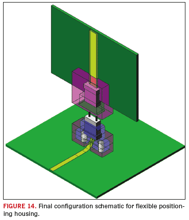
A conceptual schematic for this housing is shown in Figure 14. Balancing daughter board insertion forces with latching of electronic and optical connections requiring a zero air gap are a challenge, and important step in achieving low loss connections with multiple insertion capability. Capitalizing on the bend flex capability inherent with some waveguide films enables the required flex as the daughter board is inserted. In addition, the bending capability has opened opportunities for through-hinge connectivity for cell phones and lap top computers. Alternative techniques using a lens-to-lens coupling at the daughter board-to-backplane optical interface allows an air gap for more forgiving positioning.
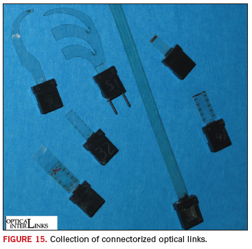
In Type Five, waveguide film edge ferrule couplings are used with self-supporting links and/or stand alone functional devices. Arrays of single or multi-layer waveguides are precisely centered or positioned within the ferrule. Figure 15 shows several MT ferrule connected flex jumpers and board edge substrate links that are fully inspected and ready for installation.
The critical connectivity issues for this type include alignment, precision, and coupling issues as previously described.
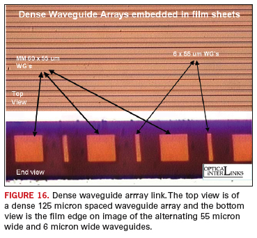
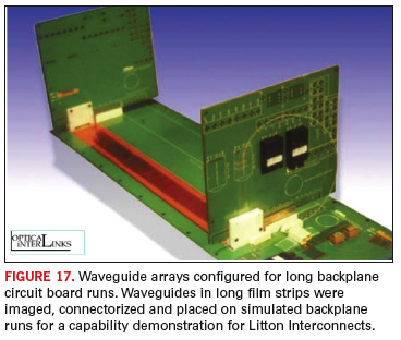
In addition, backplane/motherboard waveguide array interconnects have been created with high density waveguide arrays in a 40 cm long backplane demo interconnecting two daughter boards. The 47 cm waveguide optical path including 7 cm for the daughter boards had multiple connections operated within the loss budget of 15dB. The flex circuit shown in Figure 1 with the waveguide top and end view shown in Figure 16 was attached to a substrate for the demo board shown in Figure 17.
There are other interconnection variations for direct fiber or waveguide attachment schemes demonstrate novel butt-couple configurations between waveguides and semiconductor laser sources. Practical connectivity is achievable through the versatility provided by using self-supporting, precisely machined, stable film structures. These custom interconnects enable an extensive range of applications.
One of the most critical components to successful adaptation of optical interconnects is functional interconnectivity. This pertains to parallel links for distributing signals, as well as the distribution and or combining of signals. There is increasing interest for both substrate-based connectivity as well as for stand alone devices. High-resolution imaging and processing capability is required to create these planar polymer waveguide couplers (splitting, combining, and multi-input-to-multi-output distribution star) and multiple re-routing capability for parallel links through crossovers. The waveguide configuration at the splitting point where waveguides come together or separate must be as sharply defined as possible to avoid scattering light as it splits, combines, or is separated into multiple waveguides. Figure 18 shows the tree branch splitter with a magnified sharply defined split junction and its final packaging in Figure 19 where we spliced the 16 outputs to fit as an 8 over 8 output into a standard MT ferrule. MT ferrules at standard fiber 250 micron spacing can only fit 12 guide channels in a single row. An 8 to 1 combiner for 8 different wavelengths and one fiber coupled output made for OptiComp is shown in Figure 20 with a magnified insert shown the sharply defined 8 combining and splitting junctions as the light enters and leaves the mixing region.
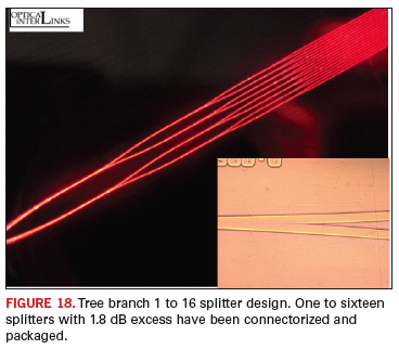
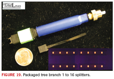
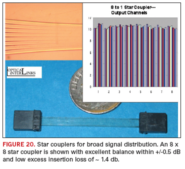
To create these sharply defined regions using other guide forming processes would seem to be very difficult to achieve. For these techniques the polymer has to be removed and/or backfilled without leaving bubbles or voids that scatter light between sharply defined smooth walled joining/splitting waveguides.
To achieve extremely low loss crossovers to re-order parallel links, photo image created low refractive index unexposed regions inside the multimode waveguides are created that enable actual waveguiding in the crossing region as opposed to no waveguiding which is standard with some other waveguide types. Thus with the low index regions defining the light path thru the crossover light is not scattered out of the guide while traversing the unguided area where the other guide is crossing. These small low index waveguide feature capabilities enable extremely dense close spaced guide arrays and are also expected to be exploited for other applications such as novel optical sensor read heads.
Critical connectivity issues include functional interconnectivity within planar waveguide links on substrates or as flex jumpers. The devices can be embedded within the link so that connectivity would be identical as the parallel link configurations with MTs, mirrors etc. above. Functional interconnectivity as stand-alone units connectivity can be achieved with similar MT style ferrules with the same constraints and tolerances for pitch and runout and for NA and guide size when interfacing with fiber arrays. For single inputs simplified fiber alignment and support structure are created to robustly lock the single fiber to the waveguide. For example the stand alone 8 to1 combiner in Figure 21 had tapered waveguides with good coupling to single fiber. The form factor for these devices is small and compact with excellent performance for excess loss and good balance.
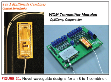
These functional configurations demonstrate practicality for a number of stand-alone or substrate attached applications that can be realized today.
So the lingering question, what is truly needed for an interconnection system to be considered practical and sufficiently developed or mature to warrant application and deployment in real world systems?
This article has reviewed and discussed the following areas.
1) The generic capabilities and requirements for practical OE substrate connectivity.
2) Polymer waveguides and the processes for creating and using them as a leading candidate of choice for daughter board OE component connections.
3) Connectivity application options and examples for reducing them to practice with associated connectivity issues that need to be considered along with potential for functionality.
To facilitate practicality, design engineers must address the entire OE substrate connectivity requirements including; performance, lifetime / survivability / reliability, and cost issues making trade offs for each specific application depending on whether low-end consumer or high-end performance is required. These system design items involve:
System attributes to satisfy the current performance requirements. Do the resulting optical electronic interconnections meet all the system performance requirements including links, functionality and loss and are they competitive with alternative technologies? Significantly different performance trade offs exist between for example low-end consumer, reliable high volume low cost automotive, and high-end military or space related applications that must be addressed by system designers. Much of the discussion above attempts to address performance and design option topics.
System attributes over time – survivability / reliability / lifetime. Does or can the optoelectronic systems continue to meet performance requirements over the anticipated service lifetime for the particular application? The application specific variables to be considered are extensive. For example, some important items are operational conditions such as temperature cycling and max/min limits, vibration, solvents, environmental tolerance issues like dirt, moisture, lifetime aging/ stability (Arrhenius plot projections for loss increases over time at temperature), consideration of relative CTE variations within the system, optical power limits vs. the application, effective polymer Tg versus packaging, RAD hardness against anticipate levels to be encountered, etc. and even standards compatibility.
Systems partitioning is an important architecture consideration for design tradeoffs that is often facilitated by photonic interconnections. Physically separating system segments can in some instances enable distributed architectures that would not be possible electronically. The net effect can be to preserve or enhance system bandwidth and reduce power drain. Sub-system interfaces can be designed more predictably enabling diverse vendors’ products to be implemented in the system. Optically multicasting signals opens the door to system designs whose performance can be scaled without changing system architecture. Optical interconnectivity enables partitioning and thus provides system design freedoms enhancing performance.
Manufacturability and costs for the entire system application. Can the system be manufactured cost effectively, reproducibly, and be functional and cost competitive with alternatives? Important processing time and costs include material processing, filtration, and purifications. It is important to ensure adequate lifetime when the polymer mix is not yet coated and when pre-coated on final or temporary substrates before exposure. Pre-exposure shelf life stability is important so that sufficient fully prepared, reproducibly performing and quality controlled materials are available to support volume manufacture.
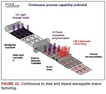
A conceptual design for a reel-to-reel process that could be altered to a step and repeat process shown in Figure 22 is suggestive of how high volume manufacture could be achieved. Equipment has been designed and demonstrated elsewhere for related polymer processing using exposure chambers and scroll ovens for final cure to maintain high throughput. Once imaged and fully crosslink/cured, waveguide films have continued to perform according to specifications even after 16 years under normal lab conditions.
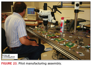
Can the entire process be amenable to scale up cost effectively? Waveguide process technology is readily amenable to producing over a hundred square feet of waveguide imaged films per 8 hour shift. Precision machining and assembly are the dominant costs in the current pilot and prototype development stage. Reducing these costs in manufacturing scale up is now being addressed. Development and operation of small scale pilot manufacturing shown in Figure 23 is underway for the Stratos Optical Technologies TxRx packaged link described previously.
The approach discussed in this article where the value of quality controlled waveguides fully processed and ready for connection before installation saves time, adds versatility and reduces potential yield loss as was discussed, resulting in an opportunity for a minimum cost high performance product. All final assembly variables must be considered including OE system assembly, IR solder reflow, cleaning solvents etc. with quality control along every step of the way. Finally the ultimate bottom line is the cost acceptable for the completed system for the applications intended?
Summary
Optoelectronic substrate connectivity is sufficiently advanced, practical and available for consideration in near term applications. For many in the industry, the evolution of optical interconnectivity at the substrate level is sufficient to begin initial prototyping. Technologies continue to develop and improve, opening up new application opportunities. We believe that the approaches outlined in this article suggest that the creation of self-supporting polymer waveguide structures are both achievable and cost effective for many applications. PCD&F
Dr. Bruce Booth is president, founder and CTO of Optical Interlinks. He can be reached at This email address is being protected from spambots. You need JavaScript enabled to view it.. Jack Fisher is a consultant at Interconnect Technology Analysis. He can be reached at This email address is being protected from spambots. You need JavaScript enabled to view it..
Acknowledgements
The authors appreciate the useful suggestions and comments from Silvio Bertling of Parker Nelco, Diana Williams of Rogers Corp., and Dale Murray of W.L.Gore as well as the extensive help in editing and organizing from Kevin Hair of Optical InterLinks.


