Metric Pitch BGA and Micro BGA Routing Solutions
For designers, working with metric units increases performance and overall quality.
The following paper provides via fan out and trace routing solutions for various metric pitch BGA (Ball Grid Array) packages.
To solve the metric pitch BGA dilemma, one should have a basic understanding of the metric feature sizes for the following:
- BGA ball sizes and BGA land pattern pad construction
- BGA via anatomy
- Trace/space
- Trace and via routing grid
- Differential pairs
- HDI hole size/annular ring.
To begin, BGA pad size is determined by the ball size as seen in Table 1 [PDF format]
from IPC-7351A. It is very important to note that IPC prefers the
maximum material condition for all BGA land sizes; they do not use the
nominal land diameter, but do use the maximum land variation diameter.
IPC-7351A has a 3-Tier BGA formula for placement courtyards
that use BGA ball size to calculate an adequate placement courtyard for
BGA rework tools. If the BGA has a large ball size, larger rework
equipment is necessary to unsolder the large solder volume. With a
small ball size, the placement courtyard can be smaller as less heat is
then required to unsolder the BGA component for rework. However, the
end user may not plan to rework the BGA if it fails. In that case,
there is no need to have a robust placement courtyard.
The
BGA, like any component, needs assembly workmanship space and requires
the minimum 0.5 mm placement courtyard boundary for pick and place
machines and for the tools to manually assemble it.
Table 2 [PDF format], also from IPC 7351A, represents the 3-Tier scenario and the different placement courtyard sizes.
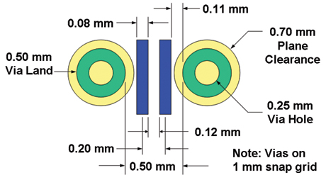
The
anatomy of the metric via is based on the 0.05 mm universal grid for
PCB design layout. The features of the metric via should always be
sized in 0.05 mm increments for the following:
- Pad size
- Hole size
- Solder mask size
- Plane clearance (anti-pad) size
- Plane thermal relief ID and OD size.
The chart in Table 3 [PDF format] represents common via pad stack feature sizes for various pitch BGA components.
The IPC-7351A LP Calculator has a BGA via calculator that
allows the user to input BGA pitch and trace/space data. It
automatically calculates the optimized via for any technology, and the
results are shown in Table 3.
Metric trace/space sizes are in 0.025 mm (1 mil) increments.
Common metric trace widths with the nearest Imperial unit in brackets (mils) are as follows:
- 0.075 mm (3 mils)
- 0.1 mm (4 mils)
- 0.125 mm (5 mils)
- 0.15 mm (6 mils)
- 0.2 mm (8 mils).
Today, the finest pitch BGA that is commonly used in the industry
today is 0.4 mm. There are plans for 0.3 mm even 0.25-mm pitch BGA
components, but mainstream fabrication facilities must first find
easier manufacture routing solutions for the 0.4-mm pitch components.
One of the reasons is that the required 0.05 mm line and space that
would be required is not yet mainstream in the electronics industry.
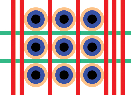
See Figure 1 and Table 4 [PDF format] for the BGA technology chart that provides through-hole via-in-land information.
|
|
For all via-in-land technology, a thermal relief on the voltage and
ground plane connections must be used to prevent cold solder joints. A
direct via-in-land connection to the plane will dissipate the heat
required to melt the solder around the BGA ball, and this will result
in a cold or cracked solder joint.
If traces are routed between pins of the BGA land with 0.4-, 0.5-
and 0.65-mm pitch, the solder mask must be a 1:1 scale to create a
solder mask defined BGA land. In this way, the traces between the lands
will be protected from exposure and possible short circuiting.
The
0.4-mm pitch BGA via-in-land through the PCB is leading-edge
technology. When laser drills are capable of producing 0.125 mm hole
sizes entirely through the board and PCB manufacturers can accurately
fill the holes with conductive material, this technology will become
mainstream.
The 0.5-mm pitch BGA via-in-land
through the PCB is also leading-edge technology. Before it can become
mainstream, laser drills must produce 0.15-mm hole sizes entirely
through the board, and PCB manufacturers must accurately fill the holes
with conductive material. However, this technology can be used when PCB
thickness is 1.0 mm or less.
The 0.65-mm pitch BGA
via-in-land through the PCB is mainstream technology. Mechanical 0.2-mm
hole sizes entirely through the board are common, and PCB manufacturers
can accurately fill the holes with conductive material. This technology
can be used when PCB thickness is 1.57 mm or less.
Microvia technology is the mainstream solution for 0.4- and 0.5-mm
pitch BGA parts when a 0.1 to 0.15 mm laser hole is drilled one or two
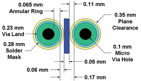
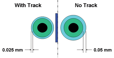
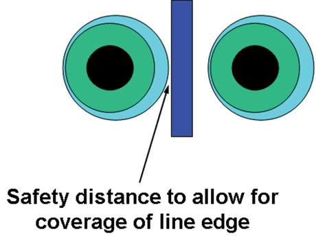
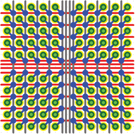
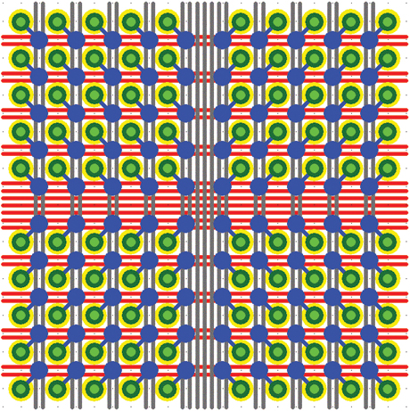
layers deep. Figures 2, 3 and 4 illustrate routing solutions for microvia technology for a 0.4-mm pitch BGA.
|
|
|
|
|
|
Whenever traces are routed between 0.4-, 0.5- and 0.65-mm pitch, the
BGA pads on the outer layers, the solder mask size and the tolerance
must be considered. It is best not to route any traces between BGA
pads, but if necessary, the solder mask should be a 1:1 scale of the
land size or a 0.025 mm minimum annular ring.
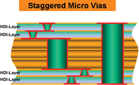
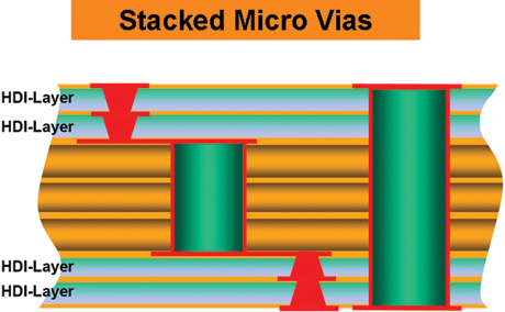
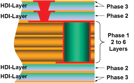
The four PCB cross-sections shown in Figures 5, 6, 7 and 8
use three different via technologies: through via, blind via and buried
via. Staggered microvias are used in Figure 5 and stacked microvias
used in Figures 6, 7 and 8. I prefer stacked microvias since PCB design
layout is easier. In this case, there are fewer visible obstacles to
manage when using the CAD tool.
|
|
|
|
|
|
|
|
Most PCB designers use blind, stacked microvias and buried vias as
the routing solutions for the 0.5-mm pitch BGA. However, the
through-hole via-in-land is actually a less expensive alternative as
long as the PCB thickness is 1 mm or less to maintain a good aspect
ratio.
Double-layer blind via technology is preferred because
layer-to-layer controlled impedance causes layer 2 to act as the ground
plane or reference plane to the layer 1 signals. Layer 3 is typically
where the signal must go. Layer 3 can then transition through the rest
of the inner signal layers using blind via technology and the layer
construction techniques noted below. This technology is for 0.4-, 0.5-
and 0.65-mm pitch BGA components.
Today, the second
finest pitch BGA in the industry is 0.5 mm. Trace/spacing of 0.075 mm
is not yet mainstream, but PCB fabrication companies are quickly
getting up to speed on this technology. The two outer rows of a 0.5-
and 0.65-mm pitch BGA are routed to a via fanout on the external layer
and blind vias, or through vias are only used on the inner rows.
Non-Collapsing Ball BGA Components
Table 5 [PDF format]
can be used for land size calculations for non-collapsing BGA balls. It
is very important to note that IPC prefers the maximum material
condition for all BGA land sizes, meaning that the maximum land
variation diameter is used; the nominal land diameter is not.
Figure 9 shows a 0.5-mm pitch non-collapsing BGA
ball. Instead of shrinking, the non-collapsing land size gets larger to
handle the solder volume that creates the solder joint. This technology
is new to the electronics industry and was created as a solution for
lead-free BGA balls.
|
|
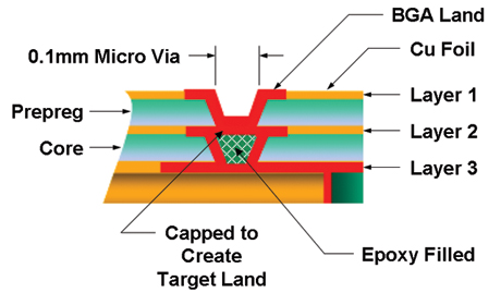
Figure 10 is a filled and capped via (Type VII
Via); a Type V via with a secondary metallized coating covering the
via. The metallization is on both sides. This technique is designed for
future via-in-land technology for 0.4- and 0.5-mm pitch and current
0.65-mm pitch BGA devices when a through-hole in a BGA land is used. It
is important to fill the via hole with a conductive or non-conductive
material. The filling material will depend on the process that the PCB
fabrication facility uses. If you call out a specific fill material
such as a vendor’s silver epoxy on your fabrication notes, the
manufacturer might have to special order that via fill material, and
this can increase the fabrication cost. This is an area where
communication with the fabricator can help determine what is the best
and most cost-effective via fill material that will meet your design
objectives.
|
|
When using via-in-land technology, solder mask is defined on a 1:1
scale on the BGA side of the PCB and tented or covered with solder mask
on the opposite side to protect the routed traces. However, you could
use 1:1 scale solder mask on both sides if you need to use the bottom
side for a test fixture.
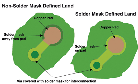
A solder mask defined land is used for 0.4-, 0.5- and 0.65-mm pitch
BGA parts when trace routing is done on the same layer as the BGA land.
The solder mask defined BGA land is only recommended when traces need
to be protected from exposure and to avoid short circuiting with the
BGA land. Also, if outer layer routing can be avoided, it’s best to use
the “non-solder mask defined” BGA technology to allow the BGA ball to
collapse around the land. See Figures 11, 12 and 13 for the various solder lands for BGA components.
|
|
|
|
|
|
The next group of BGA components is 0.8- and 1.0-mm pitch. These
components can fanout to a via placed between the BGA lands. This
fanout is the “dog bone fanout” because it looks like a dog bone with
nubs on each end. Table 6 [PDF format] lists the via size, hole size, trace width and routing grid for best routing results. Figures 14 and 15 illustrate one and two track technology between vias.
|
|
|
|
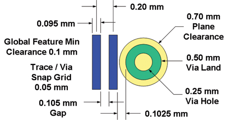
The IPC-7351A LP Calculator has a BGA via calculator that helps PCB
designers accurately calculate the trace width, trace space, via pad,
hole size and plane clearance. The plane clearance is extremely
important because it removes copper from ground planes. Ground planes
are used for return paths for all transmission lines. If the plane
clearance encroaches under a trace, the return path will find an
alternate route to return to the source. Having clean reference plane
return paths produces the fastest and quietest PCBs. By calculating the
via hole plane clearance size, the minimum copper-to-hole annular ring
can be determined, and this value is derived by the PCB manufacturer.
Fewer layers (four to six) and thinner PCB material may have a smaller
plane clearance than multilayer (eight to twenty) thick boards.
High-speed PCB layouts require layer-to-layer controlled impedance.
Differential impedance is typically 100 Ω and single-ended transmission
line impedance is typically 50 to 60 Ω. The primary goal is to keep all
the traces on a 0.05 mm routing grid and adjust the trace width
accordingly for proper impedance values. Figures 16 and 17
illustrate the 0.2-mm trace pitch; 0.05 and 0.1 mm are perfect snap
grid solutions for signal routing. You will achieve better routing
results when the traces snap to a grid.
|
|
|
|
Metric “snap grids” that produce the best part placement, via fanout
and trace routing results should be evenly divisible into 1 mm. Table 7 [PDF format] lists good and bad snap grids.
There are optimized via pad stacks that go with certain trace/space technologies. Table 8 [PDF format] illustrates the optimum via pad stack data for the three most popular trace widths: 0.1, 0.125 and 0.15 mm.
Conclusion
Using a metric placement and
routing grid and metric trace widths are far superior and easier to
work with metric pitch BGA components than Imperial unit dimensions.
Also, working with a trace route snap grid is much easier to work with
rather than using shape-based “gridless” routing solutions. The
IPC-7351A CAD library construction uses 0.05 mm as the base unit for
all CAD library land size calculation roundoffs. Clean use of metric
unit technology throughout the CAD database environment renders the
shape-based theory obsolete. When PCB designers finally discover that
working with metric units increases performance and overall quality,
they will be asking themselves “What took me so long to transition to
the metric SI measurement system?” If you complete five PCB layouts
using metric units, you will probably never go back to using Imperial
units. I guarantee it. PCD&F
Tom Hausherr is CEO & director of technology, PCB Libraries Inc. He can be reached at This email address is being protected from spambots. You need JavaScript enabled to view it..
