Award Winning Designs
An Interview with Peter Dill – 2007 winner of the Mentor Graphics PCB Technology Leadership Award.
Category: PCB design in the area of Telecommunication Switches, Network Servers, Base Stations and Computer Mainframes.Company Name: IBM Zurich Research Laboratory
Designer: Peter Dill
Design Description: Controller board for a 64x64 port high performance optical switch
The PCB Technology Leadership Awards have been around for 20 years and provide PCB designers with an opportunity to submit their best designs to be judged by a panel of experts. The categories included:
- PC Computers and Peripherals
- Consumer Electronics & Handhelds
- Industrial Control, Instrumentation, Security & Medical
- Military & Aerospace
- Telecommunication Switches, Network Servers, Base Stations and Computer Mainframes
- Transportation and Automotive
There is also an award for best overall design.
In 2007 designers came from around the world to participate, heralding from Germany, Switzerland, China, Norway, Singapore, Austria, Canada, Korea, India, Israel, Portugal, the United States and the United Kingdom.
Soft-spoken and intense, Peter Dill is a senior engineer in I/O link technology for IBM Research GmbH in Switzerland. His design wowed in the Telecommunication Switches, Network Servers, Base Stations and Computer Mainframes category. He took a few minutes to talk to Printed Circuit Design and Manufacture about the PCB design that won him a PCB Technology Leadership Award earlier this year and where he sees the future challenges for designers.
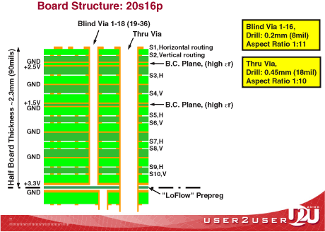
Dill said about the board, "It has 36 layers; 20 signal and 16 power/ground layers. In the power/ground layers, there are eight pairs of layers that form four buried capacity planes.” The layer structure detail is seen in Figure 1.
|
|
Dill continued, “It is a standard core technology, with no sequential lamination. The board was built in two sub-composites (layers 1-18 and 19-36) that were then laminated together. Then vias were drilled in each sub-composite that would later form the blind vias after the last lamination step has been done.”
Dill selected Isola IS620 as the laminate material because of its 3.5 Dk, loss tangent <0.01, and most importantly the high Tg of 215°C. Dill commented that the high Tg would result in a much lower risk of fractured vias.
Electrically there were three I/O technologies used: LVPECL, LVDS, and LVCMOS. LVPECL and LVDS run as 100 Ω differential pairs on the inner layers (embedded striplines), whereas the less critical LVCMOS run as single ended signals with an impedance of 60 - 70 Ω on specific inner layers and on outer layers.
Lines/Spaces in µ on differential pairs on the inner layers: 100/140 and 100/115.
Single ended outer layers: 200/200. Single ended inner layers: 150/100
The overall board statistics are:
- Number of components: 3644, with a total pin count of 42142. No embedded
- parts.
- 7 FPGAs with 1704 pins, 1 FPGA with 1020 pins, both with a pitch of 1mm.
- 40 connectors with 285 pins each.
- Number of through holes: 9188
- Number of blind vias: (1-18 & 19-36): 36053
- Number of nets: 12954 (29246 connections)
- Number of differential pairs: 4072
- Total trace length: 2.6 km
Constraints
This was a controlled impedance design with all balanced pairs at 100 Ω differential, all single ended timing and synchronization lines 50 Ω. All impedance controlled tracks run as embedded striplines. The result was 86 signal classes, describing clearances, especially class-to-class, thus keeping crosstalk to an acceptable level.
The were a total of 497 timing matched sets, describing timing constraints within a signal bundle on the one hand, and between signal bundles on the other hand. Most of the "bundles" consist of 12 differential signals.
Design Challenges
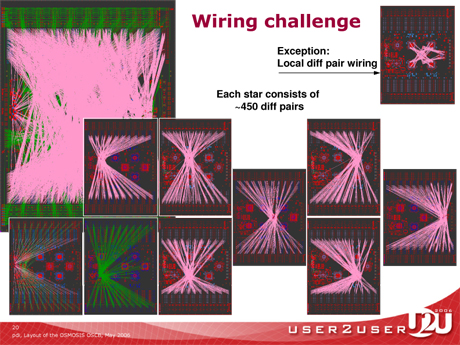
According to Dill, one of the biggest challenges was routing of 4072 differential pairs. The routing of the resulting 11000 nets that are arranged in 9 highly overlapping global stars going from the FPGAs to 40 peripheral connector locations (seen in Figure 2) that where difficult to route. The structures had nothing to do with each other yet needed to share a common space. Dill used a constraint editor to help manage the complexity. In the schematic phase he loaded in all the constraints for the individual bundles as well as the overall systems timing rules. The editor helped to develop the 86 signal classes and the design was on its way.
|
|
When asked about the specific design challenges this particular board presented, Dill replied, “Due to the high number of nets, and in particular the number of differential pairs, we decided to have the entire design including fan-out of the large BGAs automatically routed (except a few areas, such as master clock PLL and clock/sync distribution).” He continues, “I had to break down the whole job into some 12 tasks, and manually (by means of obstructs) guide the autorouter in order to achieve a result as reasonably as possible. The sheer number of differential pairs combined with the multiple star topology brought the routing engine to its limits, therefore the single routing tasks had to be broken up again into various sub-tasks.” Dill admitted, “The challenge was, to find the best sequence to facilitate the work of the autorouter, which was only achieved after three failed attempts.”
When asked what he thought was the next big challenge for the design community Dill commented that high-speed and high data rate transmission were certainly at the top of the list. Dill feels that the next big challenge is in the ultra high-speed arena where the three domains of chip, package and PCB merge and constraints will need to follow the current across the entire circuitry platform.
This is going to be a big challenge for the designers in these domains and Dill feels that we may need a new language to facilitate the interface between chip designer and packaging / PCB designer.
As the signal speed increases it will become increasing difficult to isolate the design domains. What we previously handled by a simple “over the wall” toss – will need the attention and creativity of many designers, sitting at different location and most likely working for different companies. This will take creativity and trust.
At 2Gbits/sec. and beyond domains can’t be isolated because the current is moving too quickly. We’ll need to figure out a way to design the entire pathway from chip to PCB to insure disruption free signal integrity.
“Peter’s board was one that pushed the envelope of both technology and tools,” stated Henry Potts, vice president and general manager of the systems design division, Mentor Graphics. “His innovative use of the FPGA/PCB design collaboration capability and our multi-processor auto-routing, certainly got the attention of the judges. It is boards like this that continue to push us to develop more innovative approaches to PCB systems design.”


