Solder Mask Challenges for New HDI Designs
LDI exposure holds promise to reduce or eliminate solder mask in hole issues.
We have watched the handheld market embrace HDI to reduce form factor and enable enhanced features without increasing the size and weight of the devices. Within the last few months, it has been discussed at the IPC Intel Technology Interchange and the IBM PCB – Organic Substrate Symposium how these companies, which have significant influence upon PCB technology, are moving toward HDI (high-density interconnect) technology for mainstream products. This shift in design technology will significantly increase HDI penetration in routine designs and fabrication.
Virtually all higher-technology PCBs use liquid photoimageable (LPI) solder mask. Now that HDI is about to become much more prevalent, IBM and Intel among others are asking if current LPI technology is compatible with the move to HDI. HDI technology requires smaller holes and feature sizes, and tighter registration tolerances – each of which, independently, can be a challenge, and when taken together can stress traditional LPI solder mask capabilities.
When considering the typical chemical, thermal, electrical and mechanical properties of LPI solder masks, there are no burning issues where immediate improvement is needed. HDI with existing solder masks has been used successfully in the handheld and consumer markets for years. However, as this technology is further implemented, some of the needs that have been expressed for base material properties may surface for solder masks.
Examples of improvements needed for physical properties of base materials include higher Tg and lower CTE. These are related to reduced stress, especially in higher temperature lead-free soldering processes that could cause PCB warpage or cracking. Better warpage resistance is needed especially for organic chip substrates due to their typically thinner constructions and the trend to use thinner silicon wafers that crack more easily. Improvements in crack resistance and fracture toughness of materials would also be beneficial to long-term reliability. Electrical properties that would benefit high-frequency PCBs include lower dielectric constant (Dk) and loss factor (Df).
HDI Construction Techniques
Many new HDI designs include multiple build-up layers on each side of a core or coreless constructions. Compared to conventional build-up panels with rigid, reinforced cores, HDI panels that are coreless or have very thin cores will increase scaling issues. It will be a significant challenge to maintain dimensional consistency of panels built in this manner; laser direct imaging (LDI), with its dynamic scaling capability, will become necessary to pattern the photoresist for successive layers with acceptable yields. Tight solder mask registration tolerances will require that the mask also be exposed with LDI. Traditional photolithographic exposure processes are not expected to be capable of imaging solder mask to the required registration and positional accuracy.
Another developing construction technique is to use stacked vias in each build-up layer that have been either plated shut or filled with an organic or metallic material to form a planar surface for subsequent layer fabrication. PCBs fabricated in this manner can dramatically reduce or eliminate through-holes and will have a significant impact upon solder mask processing.
An interesting possibility for solder mask imaging results if panels are built without through-holes. By eliminating the need to clean out holes, it is possible to use a non-photoimageable mask. The panels could be completely coated with solder mask, which would then be laser-ablated from the attachment pads. With the registration and scaling capabilities of LDI exposure, this technique would virtually eliminate solder mask registration and resolution issues.
Solder Mask Coating
Applying solder mask to panels is becoming a more difficult task as high density designs have 1) very small holes, 2) fine solder dams and 3) very tight registration tolerance requirements. These needs tighten the fabrication processing window considerably.
Getting solder mask out of holes does not only depend upon the development process. If less solder mask is introduced into holes during coating, it will be easier to develop the holes clean, permit lower exposure energy and will require less artwork modification. Double-sided screen printing, when properly maintained, introduces little ink into holes. Some fabricators use spray or curtain coating applications, which tend to put less mask into the holes, but these methods introduce another set of issues such as higher VOCs, dilution control, sagging, coverage of high circuits, a smaller process window when tack drying with IR ovens, etc.
Ink jet coating applications have been touted as coming technology in many areas including solder mask because it is an additive process with no development step and associated waste stream. However, ink jet solder mask coating will be a significant challenge because the ink must flow well to fully encapsulate the circuitry (especially when circuits are overetched or mushroom-shaped) and, at the same time, not flow near pads and in fine features. Specific circuitry coverages require higher volumes of ink compared to legend applications, which simply need color contrast.
Solder Mask Exposure
Both Intel and IBM pointed out that the introduction of HDI technology solder mask registration – the positional accuracy of the image compared to the panel – is a key gap. Scaling the solder mask image to the PCB outerlayer image is a significant component of registration. When discussing registration, two other parameters that go along with registration are resolution – the ability to produce fine features – and reproduction – the ability to reproduce the specific feature size from an artwork image or digital file.
Table 1 [PDF format] shows some representative changes in PCB dimensions required in the near future for HDI designs with their accompanying reduction in BGA ball pitch. These requirements lead to specific challenges for solder mask including small spaces between circuits and adjacent pads that create very tight registration requirements for pads and test points – down to as low as +/-20 microns and the imaging fine webs – from 120 microns down to 80 microns or less. The small spaces make reproduction of artwork dimensions critical to avoid solder mask on pads. These challenges will be difficult, if not impossible to meet at high yield with traditional photoimaging and registration technology.
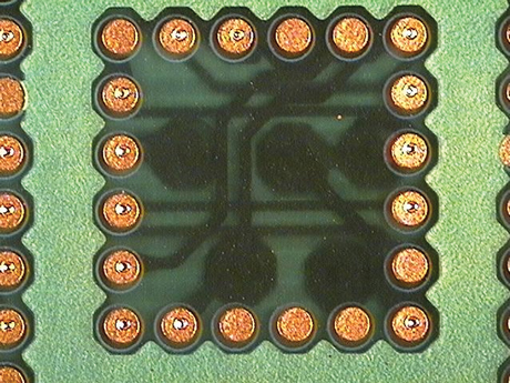
Solder mask registration is a gap for board fabricators as they attempt to build HDI designs at high yield and low cost. Traditional manual registration, whether it is pin registration or eye alignment, is capable of +/- 75 microns in production at best. Some fabricators claim they can produce panels with +/- 50 micron registration accuracy (Figure 1), but this is typically in small volume with special handling, and may be on small panels. Industry needs to get to +/-20 microns on large panels for new HDI designs.
|
|
Optical registration (e.g., two- or four-camera systems) with conventional phototools can improve upon eyeball or pin registration to some degree. But scaling issues, especially with large panels – 18 x 24 inches or larger – restrict how tight the registration can be. With traditional exposure, image scaling is done on a lot basis, with one scaling factor used for the entire lot. There is no provision for dimensional changes within a lot. And, each lot often requires a different scaling factor. Neither traditional nor optical registration addresses issues brought about by the effects of changes in temperature and humidity in a conventional exposure process and room environment.
A significant limitation to all registration techniques relates to the ability to cleanly develop solder mask from holes. Typical eye alignment and optical registration of the solder mask image is to the outer layer circuitry image, and therefore, not necessarily to the holes. Very small drilled holes exhibit a certain amount of drill wander and can cause breakout if outerlayer pad sizes are too small. Any amount of light introduced into the solder mask inside the hole during exposure will make the mask extremely difficult or impossible to be developed from the holes. Pin registration uses drilled holes to locate the image to the holes instead of the outerlayer image and, therefore, places much more demand upon the outer layer image registration to the holes to avoid mask on pads.
|
|
|
|
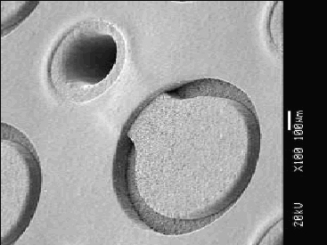
Resolution, which is the ability to produce fine features such as solder dams or “webs,†is inherently limited with traditional exposure, which typically uses a relatively non-collimated light source. Regardless of whether silver, diazo or glass artwork is employed, the image on the artwork is held away from direct contact with the solder mask in the areas between closely spaced features due to the topography of the surface (Figure 2).
The off-contact of the image from the solder mask coating can permit light infiltration under the artwork image and can contribute to image growth. And, if the fabricator uses a protective film on its phototools, it moves the image the thickness of the film that much further from the solder mask, making the challenge even greater. Image growth from light scattering or infiltration has been known to contribute to solder mask becoming partially polymerized within holes and the resulting inability to develop mask cleanly from the holes.
LDI Exposure
The best recommendation to address gaps in solder mask imaging is LDI for the exposure step in the solder mask process. LDI exposure can achieve registration positional accuracy of +/-13 microns – easily meeting the requirements for HDI designs.
LDI equipment can address scaling concerns. Because panels vary in size from panel-to-panel within a lot, and from lot-to-lot, and HDI designs require closer tolerances, artwork scaling becomes crucial if the solder mask image dimensions are to match those of the panel. With the traditional exposure process, once a “good fit†has been established, that scaled piece of artwork (or that scaling factor) is used for the balance of the lot. Panel-to-panel dimensional differences must be less than the registration tolerance or the result will be mask on pads or in holes.
An important feature of LDI imaging is the unit’s capability for scaling the digital image to the individual panel or lot being exposed. LDI equipment can scale the image to every panel individually, or measure several panels and provide an average scaling factor for the balance of the lot. This is a significant quality and productivity improvement compared to conventional exposure and permits much tighter solder mask registration. Also, when LDI is used for outer layer circuitry imaging, it increases the need for LDI exposure of solder mask to eliminate scaling difficulties.
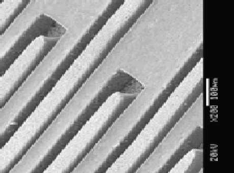
Because the laser light is very highly collimated and there are no phototools (with their associated off-contact issues), resolution of nearly 1:1 aspect ratio is possible (Figure 4), and image growth is far less of a concern.
Preliminary feedback from a large study comparing LDI to conventional imaging revealed less solder mask in holes when using LDI exposure. This confirms the reduced image growth as it relates to mask in holes because of the elimination of off-contact effects that can partially (or fully) polymerize solder mask in holes. The high degree of collimation of the laser light also inhibits light scatter into holes.
|
|
LDI exposure’s significant drawback is the equipment cost and productivity. A typical LDI exposure unit for solder mask will cost approximately $500,000 to $1 million, and can image up to approximately 25 panels per hour. By contrast, a conventional unit costs $35,000 to $40,000 and can image up to 60 panels per hour. Adding two- or four-camera optical registration can increase the cost of conventional exposure units to $175,000 to $200,000. This added cost is one of the reasons high productivity solder masks have been developed specifically to increase throughput in LDI exposure. Currently virtually all LDI capacity is delegated to innerlayer and outer layer processing, so new equipment will be required when solder mask moves to LDI exposure.
LDI Solder Masks
Solder masks, both conventional solder masks that can be exposed with LDI and products specially formulated for high productivity LDI exposure, are commercially available. Conventional and LDI solder mask processing differs in exposure time and maximum mask thickness. With LDI exposure equipment, conventional solder masks have long exposure times and may be a productivity issue (Table 2 [PDF format]). Solder masks designed specifically for LDI exposure need only 10 to 20% as much energy, so they significantly increase exposure productivity. Because LDI masks are designed to function best at lower exposure energy, they work best with thinner coatings. With HDI designs, this is typically not a limitation because these designs have low circuit height, and a thick mask is not needed to cover high circuits.
LDI solder masks have the same final properties as conventional solder masks and are RoHS-compliant and lead-free compatible. However, there continues to be a potential gap for fabricators as they process solder mask on their highest density designs. The gap is due to the demands of three processing constraints being balanced simultaneously. First, it must be ensured that all the mask is cleanly developed from small holes. Second, fine solder dams or features need to be preserved. And last, solder mask-to-feature spacing must be maintained, including keeping solder mask off pads. This can also be important for final finishes such as ENIG, where very close tolerances can result in poor catalyst rinsing, resulting in background plating.
LDI exposure with its best-in-class positional accuracy and image reproduction will give fabricators the best chance of producing these designs with high yield.
The ‘Hole Problem’
As holes get smaller, the development process must be more aggressive – generally, a longer time in the developer chemistry – to develop all solder mask from the holes. To withstand the more-aggressive development, the exposure energy must be increased to enable the fine features to survive.
When energy is increased, image growth results and fine features become larger, reducing the mask spacing to features, and can lead to mask on pads and in holes. Therefore, the artwork feature size often must be adjusted so the image does not grow onto adjacent pads. Then, exposure may need to be taken even higher so the finer features still survive development. This balancing or “process optimization†is routine for most fabricators as they produce higher technology boards, but it does narrow their process latitude. LDI exposure, with its better positional accuracy, image reproduction and reduced image growth, holds promise to significantly reduce or eliminate solder mask in hole issues.
Conclusions
Extensive implementation of HDI with high numbers of build-up layers, thin cores and coreless constructions will increase solder mask registration challenges. Higher technology designs are reaching the limits of conventional exposure processes, and new exposure technology such as LDI will be required to manufacture new designs.
Materials and processes for successful solder masking of HDI designs are available now. In the future, there are some electrical and physical properties where improvements may enhance performance and reliability, but are they not mandatory at this time.
High volume LDI production will require fabricators to make significant equipment investment for solder mask exposure. Some exposure devices under development may also enhance registration and scaling, but these are in relatively early stages of development, and marketing and comparison data are not available. PCD&M
David Vaughan is marketing manager for Taiyo Americas, Inc. He can be reached at This email address is being protected from spambots. You need JavaScript enabled to view it..


