PCB Database Viewing for SI Analyses, Parts 1 and 2

Signal integrity modeling, simulation and measurements can demand frequent examination of PCB databases.
This article ran in two parts in the August and October issues. Both parts are included here.
During
high-speed PCB design, the need frequently arises to view the PCB
database for signal integrity objectives; for instance, to ensure the
widths and lengths of routed traces are consistent with routing
guidelines (constraints) generated via simulations. It can also prove
beneficial to inspect the PCB prior to extracting the database for
post-route simulations. Another occasion that necessitates careful
database viewing is for identifying locations and net names of PCB test
points for laboratory probing and measurements after board fabrication.
A high-speed digital design team1
may include specialists in different fields such as logic design,
product design, signal integrity, EMI, mechanical engineering and PCB
design. Such a diverse and complex design environment creates the need
for the SI engineer to regularly examine the PCB database at different
stages (i.e., when the board is partly routed, completely routed or
after fabrication).
The PCB database examples in this
column employ Cadence Allegro design software, but the signal integrity
concepts apply to boards produced with other PCB programs. Williams2
is a good reference. It presents a listing of numerous PCB design
programs. Williams uses CadSoft Eagle software for several reasons,
including availability of a useful free version, relatively inexpensive
upgrades, a comprehensive library, and Windows or Linux capability.
When
selecting a PCB design package, ensure that the software can output
Gerber files (hence, avoid programs that output only to proprietary
formats or require use of a particular PCB fabricator), has
extensive/expandable part library, and an efficient autorouter feature
(for instance, a rip up/retry router can perform well, whereas a grid
router type is usually less effective2).
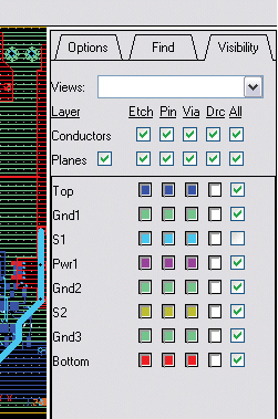
Some useful information obtainable when viewing a PCB database are the stackup layer names. Figure 1 displays the name of each layer for an eight-layer board examined with the Allegro Free Physical Viewer.
|
|
Let
us briefly consider the application and significance of layer names and
PCB stackup in producing accurate board simulations. A modern approach
to high-speed PCB design involves extensive use of EDA tools1,
modeling and simulation. One such tool is Mentor’s XTK. XTK simulations
require creation of numerous files, one of which is the Global Control
File (.GCF). It is composed of several sections: Design, Defaults,
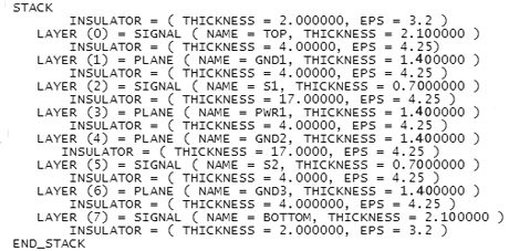
Control, Constants, Files, and Stack3. Figure 2 shows
the Stack section of a .GCF file applicable for nominal simulation of
the aforementioned eight-layer board. Stack layer names (i.e., TOP,
GND1, S1, PWR1, GND2, S2, GND3, BOTTOM) in Figure 2 are the same as
layer names in Figure 1. Figure 2 also contains thicknesses for each
layer.
|
|
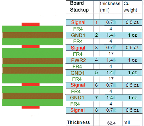
These
layer thickness values needed for accurate XTK simulations are usually
obtained from the board stackup diagram (or spreadsheet) as illustrated
by Figure 3. Here, thickness of top and bottom
(outer) layers are given as 0.70 mil (0.5 oz), which represent values
before plating. The thickness of outer layers after plating can
increase to ~ 2 mils. The (total) PCB thickness is about 62 mils, a
standard value. Other standard PCB thicknesses are 39, 93 and 125 mils.
PCB stackups are typically constructed by alternating layers of prepreg
and core. Prepreg is uncured fiberglass-epoxy resin, which becomes
cured (hardened) when heated and pressed. The core is a thin piece of
dielectric (cured fiberglass-epoxy resin) with copper foil bonded on
both sides.
|
|
Regularly,
the need arises to highlight a single-ended line, a differential pair
or a group of nets for various types of inspections. Allegro Free
Viewer allows two ways of highlighting a net: a) temporarily, using the
show element4, and b) permanently via the hilight command, which requires dehilight to be turned off. The shadow mode can be used to make highlighted nets stand out.
For high-speed PCBs, it is often advantageous to specify small trace widths in order to minimize board real estate5
and manufacturing costs. Avoid multiple vias along high-speed nets.
Subsequently, single-ended (or differential) traces are examined for
width, length and number of vias on the net.
A differential pair can be highlighted and inspected for imbalances6
that may cause electromagnetic radiation. The length difference between
traces of a differential pair can demand evaluation, because achieving
length matching (within a specified tolerance, such as 10 mils) can
prove critical for optimum timing margins7, common-mode signal prevention and EMI.
|
|
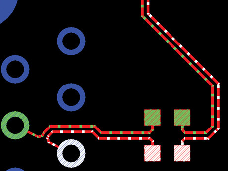
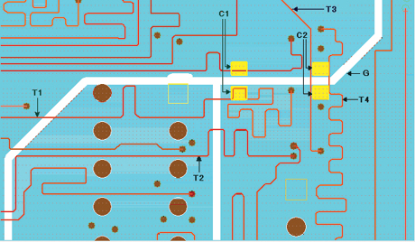
Figure 4 shows a section of a high-speed differential pair, which includes pads for AC coupling capacitors. Some high-speed links such as PCI Express8 have AC coupling capacitors, specify using individual 0603 (or a package with smaller lead inductance) capacitors and avoid the use of capacitor packs (C-packs). Capacitor pads should be implemented symmetrically for both signal lines of the differential pair. When viewing a high-speed PCB database, it is important to ensure that such bus specifications are satisfied.
High-speed differential
pairs, traces traversing reference plane splits, BGA escape regions and
relative routing of adjacent signal layers are frequently inspected for
SI objectives. Differential nets are often closely examined due to
their prevalence and significance in high-speed PCBs. For instance,
they are evaluated for length matching7, and other factors that can cause skew9.
When a differential pair includes termination resistors, DC blocking
capacitors, via pairs or serpentine sections, it needs to be checked
that such elements are implemented symmetrically10,11.
Sometimes a PCB design needs to be inspected for high-speed traces crossing slots12 in a neighboring power/ground plane. An example is illustrated by Figure 5.
It displays several traces close to and routed over splits in the
reference planes. This may cause impedance discontinuities, crosstalk
and other undesirable effects12. Figure 5 also shows
stitching capacitors aimed at reducing the adverse effects associated
with high-speed traces crossing plane cutouts. This PCB database was
evaluated using the Allegro Free Physical Viewer, by turning on the
desired signal layer and its reference plane with other layers turned
off.
|
|
The Allegro viewer can be utilized to open board files having .brd extensions. Its menu and toolbar are depicted by Figure 6.
It contains file Open, several zoom features (such as Zoom Points, Fit,
In, Out, Previous), Color (and visibility), Show Element, Measure,
Hilight, De-hilight, Grid Toggle, Rats Toggle, and Help.
|
|
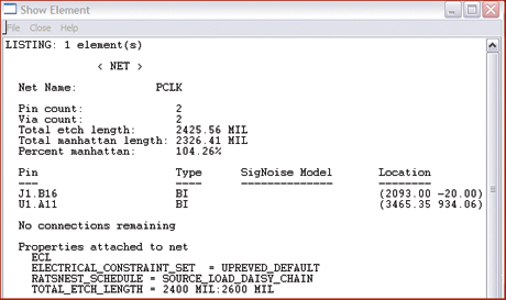
One application of the Show Element feature is to ascertain trace lengths, as illustrated by Figure 7.
The
Show Element window (Figure 7) displays the total etch length, the
percent and the total Manhattan lengths. The Manhattan length defines
the shortest path13 between two ends of the connection if
routed orthogonally. In addition to net length, the Show Element window
can reveal other information such as trace widths and
properties/electrical constraints associated with the net.
|
|
It
needs to be noted, when viewing nets with series components such as a
resistor or a capacitor, that the trace can have sections of different
net names. For instance, a clock line with a driver U1, a series
resistor R1 and a receiver U2, may have a short section (from pin of U1
to one pin of R1) with net name CLK and a long section (from the other
pin of R1 to pin of U2) named CLKR. The CLK and CLKR segment lengths
then need to be added for calculating the total trace length. When
inspecting such multiple sectioned nets, it can also prove beneficial
to review the schematic drawing of the design to gain a more clear
understanding of components and topology.
The
wildcard character (*) of Allegro Viewer can be utilized for various
applications. For instance, it is possible to simultaneously examine a
family of nets and to ascertain the min/max routed lengths for a group
of traces belonging to a bus. The zoom and pan features of this
software can be applied to closely inspect various PCB features
including long nets.
As mentioned in Part 1, the
examples in this column utilize Cadence Allegro; however, similar
inspections and SI evaluations are feasible on databases produced by
other PCB design programs.
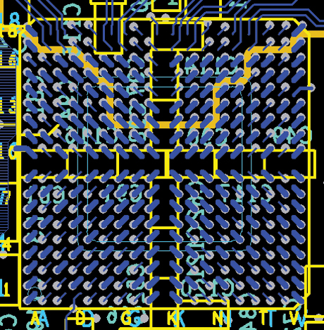
Several features of BGA breakout as depicted by Figure 8
deserve appraisal. Connections between differential pairs and BGA
balls, the necking down of traces, which can cause impedance
discontinuities, and power delivery to the chip usually demand
inspection.
|
|
It
is desirable that traces routed between neighboring pins (or vias) be
properly centered and to avoid routing over plane splits (and other
plane voids such as anti-pads) whenever feasible.
BGA escape regions often routed in a radial14
fashion (out from the center of the land array) can produce a
horizontal and a vertical slot useful for placing surface-mount
decoupling capacitors on the bottom layer. It also allows superior
power feed (wider power channel) to the BGA.
It is often necessary to identify test or access points for oscilloscope probing and signal measurements. Some standard1
SI measurements include: rise/fall times, propagation delay, noise
margin, timing budget, overshoot/undershoot, and crosstalk. A suitable
access point for probing is often on the bottom layer underneath the
BGA at a dog-bone via. A ground close to the signal pin is also needed
for probing to minimize ground loops and associated inductive noise
when applying oscilloscope probes15.
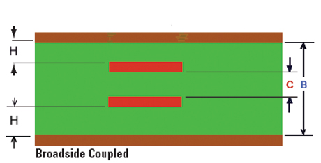
When the PCB stackup includes two adjacent signal layers such as dual (or broad-side-coupled) stripline structure as shown in Figure 9, it is sometimes necessary to evaluate the routing.
|
|
Figure 10
displays numerous nets belonging to two such adjacent inner layers. In
certain regions, the traces of the two layers are routed parallel, and
in other areas, they are orthogonal to each other.
|
|
For high-speed PCBs, it is preferable that signals on adjacent layers16,17
be routed in an orthogonal (90 degree conductor crossing) fashion to
minimize crosstalk. However, coupling would also depend on such factors
as separation distance between the layers, the parallelism length,
driver strength and signal edge rates. It is preferable (for
diminishing crosstalk) to place the signal layers close to the
reference planes, to use thin trace widths, short parallel lengths and
offset the traces. The exact magnitude of crosstalk can be ascertained
via modeling and simulation.
An outstanding resource for exploring additional information related to topics discussed in this column is the Signal Integrity List email reflector (SI-LIST). It is free to subscribe to the SI-LIST and the list archives are available18 for viewing. PCD&F
Dr. Abe (Abbas) Riazi is a senior staff electronic design scientist with ServerWorks (a Broadcom Company). He can be reached at This email address is being protected from spambots. You need JavaScript enabled to view it..
ACKNOWLEDGEMENTS
My gratitude to Richard Kuo, Greg Albers, Peter Arnold , Mark Furnace, and Suresh Vegesna for reviewing the manuscript and furnishing excellent feedback.
REFERENCES
1. Roy G. Leventhal and Lynne Green, “Semiconductor Modeling For Simulating Signal, Power, and Electromagnetic Integrity”, Springer, 2006, pp. 1-7, pp. 526-527.2. Al Williams, Build Your Own Printed Circuit Board, McGraw-Hill, 2004, p. 18, pp. 190-193.
3. Quad Design, Preparing PCB Design Databases for Simulation with TLC/XTK/QUIET, document no. Q3FR018MNL6_5, November 1996, Chapter 5.
4. Cadence, Allegro/APD Design Guide: Getting Started, product version 14.2, 2002, pp. 129-137.
5. Stephen H. Hall, Garrett W. Hall, James A. McCall, High-Speed Digital System Design A Handbook of Interconnect Theory and Design Practices, John Wiley and Sons, Inc., 2000, pp. 37-38.
6. Tom Granberg, Handbook of Digital Techniques for High-Speed Design, Prentice Hall, 2004, p. 711.
7. Abe Riazi, “Length Matching for High-Speed Differential Pairs,” Printed Circuit Design & Manufacture, February 2005, pp. 17-18.
8. PCI Sig, Add-in Card Compliance Checklist for the PCI Express Base 1.1 Specification” Revision 1.1, 2006, p. 17.
9. Bruce Archambeault, “EMI/EMC Concerns for High-Speed Differential Signals,” Printed Circuit Design & Manufacture, July 2007, PP. 16-17.
10. Abe Riazi, “ Differential Signal routing Requirements,” Printed Circuit Design & Manufacture, February 2004, PP. 22-23.
11. Abe Riazi, “ Avoiding Differential Pair Routing Violations,” Printed Circuit Design & Manufacture, August 2004, PP. 26-29.
12. Abe Riazi, “Effects of Plane Splits on High-Speed Signals, Part 1,“ Printed Circuit Design & Manufacture, February 2007, PP. 16-17.
13. Lee W. Ritchey, Right the First Time: A Practical Handbook On High-Speed PCB And System Design, Vol. 1, Speeding Edge, 2003, PP. 222-223.
14. Bernard Voss, “BGA Power Delivery Routing,” Printed Circuit Design, September 2002, P. 33.
15. Peter D. Hiscocks, James Gatson, “Oscilloscope Probes: Theory and Practice,” Syscomp Electronic Design Limited, July 12, 2007.
16. Leonard Dieguez and Salman Jiva, “Altera Gigabit Channel Design Guidelines,” Signal Integrity Net Seminar Series, 2007.
17. Bernard Voss, “Tricks of High-Speed PCB Stack-Up,” Printed Circuit Design, April 2002, P. 18.
18. SI-LIST archives are viewable at freelists.org/archives/si-list. Old (prior to June 6, 2001) archives available at qsl.net/wb6tpu.
