Achieving an ENIG Resistant LPI Solder Mask Process

Improving process control in the solder mask area pays dividends in increased yields.
As a fabricator, you are probably familiar with this situation. You have spent a great deal of time and money to get the boards through the manufacturing process only to see mask issues such as peeling or lifting after the ENIG (electroless nickel immersion gold) process. Obviously, this is very frustrating. The key for the troubleshooter is to understand the possible origins of the defect. Is peeling solder mask due to poor surface preparation, or an over cured mask? It is also possible that the mask is too thin, especially over the knee of the circuit. And of course, the ENIG chemistry itself may be contributing to the defect. Regardless, one must approach the problem from all angles and have a clear road to follow. As Yogi Berra once said, “You got to be careful if you don’t know where you’re going because you might not get there.†This applies to troubleshooting.
Potential Causes of Peeling
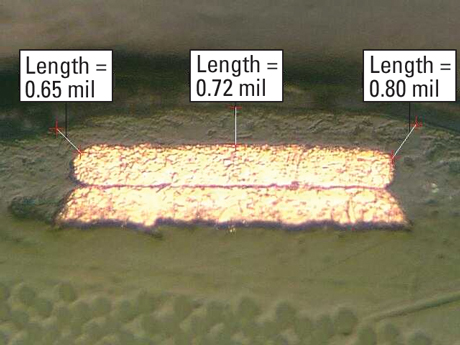
In Figure 1, the mask coverage over the copper trace is very critical with respect to the mask’s resistance to peeling. It is highly recommended that the thickness of mask over the traces, especially over the knee, be at least 0.6 mils. At a minimum, there should be no less than 0.4 mils of (dry) solder mask when processing through ENIG. Certainly, a thin coating is susceptible to peeling even without ENIG. However, one must keep in mind that ENIG is an aggressive plating process - period.
|
|
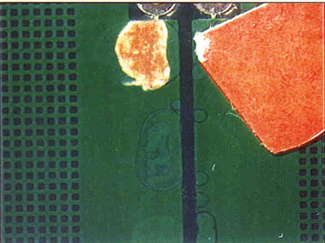
Of course, other issues arise as shown in Figure 2. The blistering and peeling of the mask either from traces or ground plane areas is quite evident. Possible causes are (1) mask thickness too thin, (2) insufficient cure temperature or time, (3) poor surface preparation, (4) insufficient tack dry, or (5) over curing of the mask. With respect to cure temperature, follow the mask supplier’s recommendations. As an example, if cure cycle is called out to be 150°C for 60 minutes, this means that the time of 60 minutes is at that temperature give or take 5 minutes. Often, problems are found with insufficient cure due to operators opening and closing the oven doors, allowing heat to escape. Tunnel ovens must be profiled on a regular basis to ensure the proper temperature is met and for the optimum time.
|
|
Despite all of the potential causes cited above, one must not ignore over curing of the mask as a possible cause. Simply stated, over curing embrittles the mask and makes the mask less flexible. It is the curing step that completes the cross-linking of the epoxy groups with the amine groups, further enhancing the physical, electrical and chemical resistance properties of the mask. However, if one measures the pencil hardness of the mask using the Wolff-Wilburn method, the indication of a pencil hardness of 8 H or greater is an indication that the mask lacks the flexibility to stand up to ENIG.
One should chose a mask with the ability to achieve a pencil hardness of 6 to 7 H. Often the argument is that a pencil hardness less than 8 H will not resist scratches due to improper handling. It has been this author’s experience that if the operators follow proper handling procedures, scratches are not an issue.
Thus for better ENIG resistance, chose a mask with more flexibility and less hardnesss. It is simply a tradeoff. It is very difficult to achieve very high pencil hardness and retain excellent stability in ENIG.
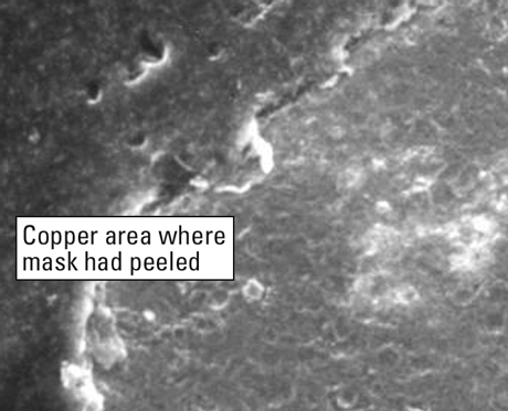
Poor surface preparation (prior to coating the circuit boards with the ink) or a contaminated surface leads to mask lifting. Figure 3 depicts a surface that was analyzed after reporting solder mask adhesion problems. It was determined from surface analysis that a high degree of aluminum was found on the copper in the area of the defect.
|
|
Upon further analysis, it was revealed that the fabricator uses aluminum oxide scrubbing as a surface preparation mechanism for solder mask adhesion. It was apparent that the excess aluminum interfered with solder mask adhesion. It is critical that after any type of surface treatment, sufficient rinsing takes place to ensure the copper surface is free of particulate matter and debris that interferes with adhesion. PCD&M
Michael Carano is vice president, marketing and business development at Electrochemicals Inc.; This email address is being protected from spambots. You need JavaScript enabled to view it..


