2007 JPCA Show Technology Summary
This year it was a one-stop show, from PCB design, to fabrication, through testing and into assembly.
Download the extended version of this article, with additional photos, in PDF format
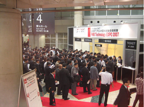
The annual JPCA Show was held at Tokyo Big Site from May 30 - June 1. According to JPCA, the 2007 show had a record attendance of 131,355 in three days (Figure 1). On the last day, 50,492 people crowded the exhibition hall. Because of the concurrent exhibition of JISSO technologies (assembly sector), the total number of exhibitors increased from 526 (1,601 lots) in 2006 to 627 (2,139 lots). This year’s theme was “Collaboration to the Next – Electronic Circuits and JISSO Technologies which support Cutting Edge Electronic Devices.†The 2007 JPCA show was a “one-stop-show†from PCB design, fabrication, testing and to assembly.
|
|
PCB Design
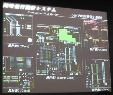
Several well-known design software companies were present such as Zuken and Dynatron. Zuken showed a design scheme in which five designers work on one PCB design concurrently in different circuit areas without interference from each other. NEC came up with a similar scheme many years ago, but “concurrent design†was carried out by only two designers. Zuken seems to have extended the “concurrent†scheme to five concurrent design schemes (Figure 2). In 2006, Mentor Graphics, Cadence and others exhibited, but they did not exhibit this year.
|
|
Base Laminate Materials
In addition to the usual Japanese base laminate makers, there were a number of Asian competitors at the show. Doosan Electronic Materials, Shengyi Electronics, ITEQ, Grace Electron, ITEQ and Ventec Electronics exhibited at the show.
Mitsubishi Gas Chemical is best known for its BT resin-based laminates. The laminator increased its total BT laminate manufacturing capacity to 1,000,000 m2 per month. Matsushita Electric Works, now “Panasonic Electric Works†is offering a variety of Megtron laminates. Megtron 6 is said to have been adopted to fabricate MLBs (multilayer boards) for IBM’s high-end servers. Hitachi Chemical’s 679 series laminates (679FG, etc.) are well accepted by IC substrate manufacturers. Sumitomo Bakelite is not known well outside Japan but it provides much of the high-end laminate in Japan.
Drilling Equipment
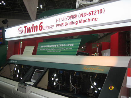
The Japanese drilling machine market is dominated by Hitachi Via Mechanics (Figure 3), although Roku-Roku and Takeuchi still sell a few machines. Takeuchi is now owned by a Taiwanese company.
|
|
One interesting exhibitor was Schmol Maschinen of Germany, which showed up for the first time at a JPCA Show. It had one installation in Japan, but it seems to have succeeded in selling two more during the show.
There were four laser drilling machine exhibitors: Hitachi Via Mechanics, Mitsubishi Electric, Sumitomo Heavy Industry and Takeuchi. There was no sensational laser drilling equipment this year. All machines exhibited showed twin-table, twin-beam systems. The world laser drilling equipment market is dominated by Japanese makers. One noticeable competitor is Electro Scientific, which specializes in UV/YAG laser systems used for flex circuits and IC substrates.
In the early days of laser drilling, the drilling speed was about 30 to 40 holes per second. Today, with twin-beam and twin-table schemes, the drilling speed is almost 2,000 holes per second for regular microvia boards. In practice, it is about 1,000 holes per second for a cell phone board and close to 3,000 holes per second for IC substrates (flip-chip). Over 4,000 laser drilling machines have been sold throughout the world in the last 15 years. Of about $8.5 billion microvia boards produced worldwide in 2006 – inclusive of flip-chip substrates – Japanese output (domestic and overseas) accounted for 45% of this figure.
Direct Laser Imaging
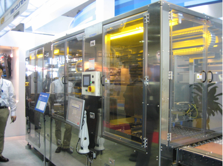
The LDI (laser direct imaging) field of imaging technology is a competition between Orbotech and four Japanese vendors: Hitachi Via Mechanics; ORC Manufacturing, which purchased the LDI business unit last year from Pentax (the remaining Pentax company is being purchased by optical company Hoya); Fuji Film; and Dainippon Screen (Figure 4). At the time of JPCA, Orbotech is said to have installed approximately 250 units cumulatively, whereas the four Japanese companies have installed about 115 to 120 units. It is estimated that at the time of the show, Japanese PCB makers have about 120 LDI units, the largest installation base in the world today. This year, ORC had attracted the largest number of visitors to its Di Impact model, which is a fully automated, double-sided imaging system equipped with a loader and unloader.
|
|
All in all, the total LDI systems sold worldwide in the last decade or so come to about 450 units, including old models no longer used. It looks like LDI systems are coming of age – finally – with heated competition.
Dry Film for LDI
DuPont, Nichigo-Morton together with Eternal Chemical, Hitachi Chemical and Asahi Kasei advertised dry-film products for LDI. It is estimated that the combined sales volume of LDI dry film by Japanese makers is about 1,000,000 m2 per month at this time and is increasing steadily. In 2006, the total sales volume of dry film worldwide is estimated to have been about 800,000,000 m2. Hence, the total LDI film sales volume is about 1.5% of the total.
Now that all the players are lined up – from dry film for conductor imaging and solder resist and five LDI system makers plus a few others (not present during JPCA Show such as SupraLight model from Bacher) – the world is ready for LDI after 10 years of protracted development.
PCB Fabricators and PCB Processes
The number of PCB fabricator exhibitors continues to decrease every year at JPCA. However, there were still more than 50 fabricators that showed up unlike other PCB shows in the world (TPCA, CPCA, KPCA, IPC, etc) with the exception of Electronica, where 104 PCB fabricators from all over the world exhibited in 2006. Samples of PCBs shown at tradeshows are the best indicators of technology trends and also good indicators of the technology level of the exhibitors. From this view, JPCA is definitely the best in the world in this author’s opinion.
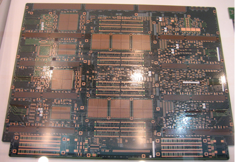
There were 42 Japanese fabricators and 14 foreign fabricators at the show. Of the 42 Japanese fabricators, Eastern, Ibiden, CMK, Shirai Denshi, Sumitomo Metal Electrodevice, Dainippon Screen, Toppan NEC Circuit Solutions Inc (TNCSi) (Figure 5), Japan Circuit Industry (JCI), Japan Victor Corporation (JVC), Hitachi Chemical, Panasonic Electronic Devices (PED), Hitachi PWB Solutions, Fujikura Corporation, Nippon Mektron, Arm Electronics, Meiko Electronics, Sumitomo Bakelite, Shinko Mfg, Dainippon Printing, etc., are good size fabricators. Many top fabricators did not show up.
|
|
Japan produced about $11.3 billion in PCBs in Japan and $4 billion overseas, or total of $15.3 billion – 32% of the world’s production in 2006. The driving force of domestic production was IC substrates, microvia boards and flexible printed circuits (FPC) and for overseas production, all sorts of boards for consumer electronics including FPC.
This year, embedded component circuit boards were quite visible, although they started to show up two years ago. Ibiden, CMK, TNCSi, Fujikura, DNP, Clover Electronics, PED, YKC and several others showed their samples. Some of then are in the advanced production stage, delivering more than one to two million pieces of embedded component circuit boards so far. They claim that their production will accelerate this year with good acceptance from their customers. Practically all embedded circuits are small-size “module†circuits for such applications as watch modules.
High layer count MLB production in Japan shot up last year by almost 40%. The total production of MLBs in 2006 with a layer count of 18 and above is estimated to be about $445 million, second, although distant, to the North American estimated production of $830 million. These technologies developed back in the mid-1980s when IBM, Siemens, Cray Research, NEC, Fujitsu and Hitachi competed in general purpose and super computer technologies. Manufacturers of high layer-count boards have been increasing their production capacity. Some of the most flamboyant package substrates are made in Japan.
As the total number of transistors in one chip continues to increase, the number of layers needed from the IC substrate package continues to increase. To ease the increase, lines and spaces are becoming narrower. I saw samples of package substrates with having 15 µm lines and spaces during various plant visits after the show. If the trend continues, lines and spaces may come down to 5 µm by 2013. This requires entirely new imaging and conductor formation technologies.
Another interesting technology was “coreless†build-up microvia boards, which includes IC substrates and boards for cell phones. It is interesting to note that with the advent of coreless structure, the demand for ALIVH and B2it boards has been increasing steadily in the last few years. Accordingly, the makers of these boards have been increasing production capacity. The total production of ALIVH and B2it boards combined was about $435 million in 2006, only about 5% of the total worldwide microvia output of about $8.5 billion, but because of the “natural structure†of filled vias, these boards have strong support in Japan. In Japan, $435 million accounts for about 14% of microvia output, not a small share.
A large portion of multilayer FPCs made in Japan have a laser drilled microvia structure to support fine-pitch components. Currently, 0.4 mm pitch is the forefront of fine-pitch CSP but this pitch is to be reduced to 0.3 mm by the end of this year for certain products such as cell phones and digital still cameras, resulting in an increased demand for microvias.
Other Topics
One of the leading makers of horizontal equipment, TCM (Tokyo Kakoki Co. Ltd), made an announcement that it has been developing a new generation of etching machines called “Swim.†In this equipment, the panel is designed to “swim†through the etching chamber without touching the wheel. TCM makes various horizontal equipment allowing 40 to 60 µm core laminates (40 µm core is actually 64 µm total with 12 µm copper foil on both sides) to be carried through.
Micro Craft presented an inkjet legend machine. The company mentioned that it has sold about 30+ units so far, slightly more than half have been shipped to Asian countries. Micro Craft and Printar are now major inkjet legend machine makers. They are joined by Orbotech through the purchase of New Systems. Printar is said to have sold about 30 units.
Recently, “printed electronics†has been drawing attention worldwide. During the JPCA show, several companies exhibited their versions of printing technologies, one of which was New Long, who is well known for fine-line screening for hybrid circuits and similar technologies. It exhibited samples of conductor screening for wafer-level packages. The screened line width shown is 30 µm. It is not in production yet, but it seems that New Long is heading in the right direction.
|
|
One final subject this author would like to touch on is small hole drilling in Japan. I have seen mass drilling of thin-core CSP (40, 60, 100 µm thick) with small diameter drill bits. For example, five stacks of 100 µm BT laminates are drilled with 100 µm drill bits at the speed of 650 hits per minute. Similarly, three stacks of 100 µm BT laminates are drilled with 75 µm drill bits at similar speed; 50 µm mechanical drilling is becoming a reality. Union Tool showed photographs of 10 µm diameter drill bits and drilled holes (Figure 6). PCD&M
Dr. Hayao Nakahara is president of NT Information and contributing editor to PCD&M. He can be reached at This email address is being protected from spambots. You need JavaScript enabled to view it..
