Modeling Frequency-Dependent Conductor Losses in Serial Data Channel Interconnects – Parts 1 and 2
Roughness on the large conductor surfaces of a PCB can increase the interconnect loss as much as 50%.
Editor’s Note: This article ran in two parts in the July and August issues. Both parts are included here.
Faster data rates in packages and on PCBs drive the need for advanced electromagnetic models both for early exploration of the interconnect budget and for serial data channel verification. Without these advanced models, the design process has to be repeated multiple times to improve overall performance, adding delays and increased costs to the project.
In particular, transmission lines require ultra-broadband models of conductors to simulate multi-gigabit data channels. Static and magneto-static 2D field solvers are typically used to design high-speed nets, but they are not quite suitable to design multi-gigabit channels due to multiple limitations discussed in this paper.
The industry is gradually becoming aware of these deficiencies, and a transition from static to 3D full-wave tools is taking place. Unfortunately, 3D and full-wave analysis does not automatically guarantee that all conductor-related effects are taken into account. Solutions originally developed for microwave applications, for instance, are being optimized for analysis of relatively narrow-band systems and for frequencies where skin effect is well developed. Such models are not valid at low and intermediate frequencies where there is no skin effect or skin effect is not developed yet, and the models have to include those frequencies for digital applications.
As a result, a broadband model of interconnects may show non-physical behavior of extracted inductance and resistance at low and intermediate frequencies or violate causality requirements. In other words, the transition to skin effect in traces and metal planes is usually neglected in 3D tools in general. The frequency-dependent skin effect is usually roughly approximated or not accounted for at all in 3D full-wave time-domain tools and in some PEEC-based tools.
Another differentiator of PCB and packaging interconnects is the large conductor surface roughness that is neglected by almost all electromagnetic and static tools. Many 3D tools do not have built-in capabilities to extract modal and per unit length parameters of transmission lines. This paper discusses the limitations of different simulation techniques for conductor effects and requirements for broadband transmission line parameters extraction tools.
Absorption of Energy by Conductors and Skin Effect
Multiconductor transmission line models are usually used to simulate interconnects in packages and on PCBs. Quasi-TEM waves propagating in these lines have electric and magnetic field components predominantly in the line cross-section, and the signal is transmitted along the line by these fields.
The fields may have components along the line if there is non-homogeneous or multilayered dielectric and also in the case of non-ideal conductors discussed here. Non-ideal conductors absorb the electromagnetic energy and cause unwanted loss and dispersion that have to be accounted for in the transmission line analysis.
|
|
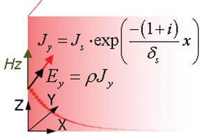
Mathematically, fields inside the conductors can be described with Maxwell’s equations without the displacement term as a magneto-quasi-static or diffusion problem with very high accuracy. Locally, on the surface of the conductor, an electromagnetic field can be approximated as plane waves transmitting the energy inside the conductor that produces non-uniform conductor current distribution as illustrated for a simple case in Figure 1.
Parameter δs of the complex exponential function is called skin depth and can be calculated as
|
|
ρ is conductor bulk resistivity in [Ohm-m], µ is permeability in [H/m] and f is frequency in [Hz]. ρ for annealed copper is about 1.724 · 10-8 [Ohm-m] for instance.
The skin depth δs becomes smaller at higher frequencies, and eventually, becomes much smaller than the conductor cross-section. We can call this state a well-developed skin effect. Note that fields and currents in conductors with complex shapes can be approximated as the superposition of plane waves from DC to any given frequency.
Qualitative View of Conductor Effects on Signal Propagation
Considering multiconductor lines, there are three major factors defining distribution of currents in the conductors and corresponding loss and dispersion. These are the conductor bulk resistivity, shape of the conductors and proximity of the conductors (strip and plane for instance).
In addition, surface roughness and dielectrics surrounding the conductors alter the conductive properties of the traces. The frequency-dependent conductor effects can be qualitatively separated into three frequency regions – low, medium and high1,2. This classification can be based on the state of current density distribution in conductors1 or on the base of properties of the conductor impedance per unit length (PUL)2. Note that any classification is necessary if only to understand the limitations of the models that include only some effects and do not take into account the others.
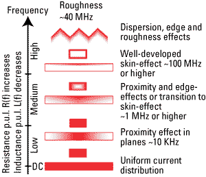
Uniform current distribution in homogeneous trace and plane conductors takes place from DC to some relatively low frequency. (It is not valid for composite conductors.) The corresponding impedance PUL has almost constant real part RDC and inductive part with almost constant inductance LDC that characterizes the uniform distribution of a magnetic field inside both strips and planes as illustrated in Figure 2.
|
|
Current distribution in conductors may start changing at frequencies as low as 10 KHz where plane current concentrates below the strip to minimize the energy absorption by the plane (though these losses grow with the frequency). At medium frequency range, current density re-distribution takes place. Corresponding effects are not separable but can be called by different names like proximity or crowding effect, edge effect or transition to skin effect as also illustrated in Figure 2.
At medium frequencies, the resistance PUL increases and inductance PUL decreases because of shrinking conductor area with the current and magnetic field. Skin and edge effects become visible at higher frequencies. Finally, at relatively high frequencies, most of the current flow in a thin surface layer and corresponding state can be characterized as the well-developed skin effect.
Without edges and dielectrics, the resistance at high frequencies grows as √f and conductor internal inductance decreases as 1 / √f. Interaction of non-homogeneous dielectric dispersion and edge or proximity effects further accelerate the growth of resistance PUL with frequency2. This is valid even for ideal dielectrics. In addition, roughness may considerably increase the resistance PUL at high frequencies3.
Transition to Skin Effect
Though conductor shape and dielectric properties may have significant effect on the energy absorption in the conductors, we will try to determine the medium or transition frequencies for different technologies that use strip or microstrip lines. This can be done on the basis of strip or plane thickness ratio to the skin depth.
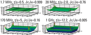
If conductor thickness is less than or equal to 0.5 · δs (half skin-depth) the skin effect is not visible as illustrated in Figure 3 for a typical PCB trace. At a frequency when the strip thickness becomes equal to 2 · δs, the skin and edge effect become visible as shown in Figure 3, but it is not well-developed skin effect yet. According to the rule of thumb in microwave engineering, the skin effect becomes well developed only if conductor thickness becomes equal to 5 · δs (five skin-depth).
|
|
Alternatively, the high transition frequency can be derived on the basis of comparison of the real and the imaginary parts of internal conductor impedance PUL2. The low transition frequency may be defined by deviation of imaginary part from zero. The transition ends as soon as the real and imaginary parts are equal with some tolerance. For the strip example shown in Figure 3, the impedances PUL are
Z (1.7 MHz) = 2.67 + i0.11, Z (28 MHz) = 2.95 + i1.71, and Z (170 MHz) = 6.44 + i6.22 [Ohm/m].
It is clear that at 28 MHz, where the strip is two skin-depths, the imaginary part is almost 40% different from the real part, and it is still a medium frequency. Note that the conductor impedance real and imaginary parts may deviate from each other at higher frequencies due to the dispersion and edge effects.
|
|
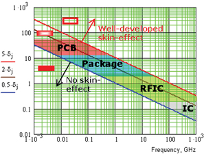
We can generalize this observation on the transition as shown in Figure 4. Strip or plane thicknesses on PCBs and in packages can range from 1 µm to 50 µm and corresponding transition frequencies range from 1 MHz to above 10 GHz.
Conductor Surface Roughness
Roughness is what makes serial data interconnects modeling considerably different from the analysis of microwave ICs for instance. Polishing of conductor and dielectric surfaces is not a possibility for PCBs, and roughness can increase the interconnect loss as much as 50% as noted in the references3.
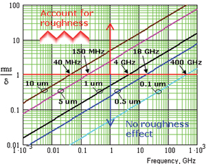
There are multiple methods developed to model the roughness, and Figure 5 provides guidelines to determine at what frequency the roughness has to be taken into account in the interconnect analysis. As soon as the roughness root mean square (rms) value becomes comparable with the skin depth, it must be taken into account. Some manufacturing technologies give 10 µm rms roughness that degrades the signal at frequencies as low as 40 MHz. In contrast, modeling interconnects with 0.5 µm rms roughness may not require the roughness models at frequencies below 18 GHz.
|
|
Static and Quasi-Static Field Solvers
A static field simulator solves Laplace’s equations for electrostatic potential in 2D cross-sections of multiconductor transmission lines. Boundary element methods with meshing of conductor surfaces and dielectric boundaries or finite element methods are usually used in commercial static field solvers. The result of a static solver analysis is always a capacitance matrix per unit length and charge distribution on the conductor surfaces. All other parameters are derived from these.
To find an external inductance matrix per unit length Lext for instance, capacitance matrix C(ε0) has to be calculated for the problem without dielectrics and then the inductance is calculated as Lext = µ0ε0 C(ε0)-1. Here ε0 and µ0 are permittivity and permeability of the vacuum. Conductors are assumed to be ideal (no resistivity) in all computations. To estimate conductor losses and conductor internal inductance, charge distribution on the conductor surface is calculated for the original problem with dielectric layers. Then, assuming well-developed skin effect in all conductors, perturbation technique is used to calculate resistance per unit length Rs(f0) at a given frequency f0 (it is usually 1 GHz in commercial field solvers). In addition RDC is calculated as diagonal matrix with resistances per unit length of all strips on the diagonal.
Finally, Wheeler’s assumption about the equality of the real and imaginary parts of conductor internal impedance PUL is used to approximate the total frequency-dependent impedance PUL as follows:
|
|
RDC, normalized skin-effect resistance
|
|
and Lext (or inductance at infinity) are all components of the conductor-related loss and dispersion models in W-element or similar transmission line models in system-level solvers. There are multiple problems with this approach.
First of all, RDC usually does not include the reference plane resistance, and in addition, it creates inequality of the real and imaginary parts of the internal impedance at high frequency, which contradicts Wheeler’s rule. Second of all, it does not capture behavior of the impedance at transitional frequencies when resistance and inductance PUL just begin to deviate from the DC values. In addition, the internal inductance goes to infinity at DC as 1 / ?f instead of converging to the inductance at DC that is basically unknown in this approach.
High-frequency approximation in problems with dielectrics is also not valid because of the current redistribution due to the dispersion and edge effects that are not accounted for in the static solution; it requires a full-wave solution. It basically explains why microwave engineers, for instance, do not use such approximation and the static field solvers in general.
To extract frequency-dependent resistance R(f) and inductance L(f) matrices PUL, a 2D magneto-quasi-static field solver can be used. It solves frequency-independent Laplace’s equations outside the conductors and frequency-dependent diffusion equations inside the conductors to model the skin effect. A hybrid technique with filaments inside the conductor and a boundary element method outside the conductor or a finite-element method are usually used to solve the problem.
Though it can model conductor current re-distribution in the transition to skin effect frequency range, the extraction or R and L at frequencies with well-developed skin effect may be computationally very expensive. A finite element or filament size in the conductor interior has to be a fraction of the skin depth at the highest frequency. Otherwise, the artificial resistance saturation effect takes place when the resistance approaches some value and does not grow with the frequency after that. To extract parameters of a line up to 10 GHz, the element or filament size near the metal surface has to be at least one quarter or a skin depth that is about 0.16 µm. It would require about 236,000 elements to mesh the interior of a 10 mil by 1 mil trace for instance, and in addition, the interior of one or two planes have to be meshed; another two million elements may be required.
Even if those limits are alleviated with a non-uniform conductor interior meshing, the solution does not include the effect of non-uniform dielectric on the current distribution or dispersion and edge effect. A magneto-quasi-static problem does not include dielectrics at all. In general, magneto-quasi-static solvers are suitable for extraction of R(f) and L(f) from DC to the transitional frequencies, but only in cases where there is not much dispersion from non-homogeneous dielectrics. Finally, both static and magneto-quasi-static solvers do not simulate the effect of roughness.
3D Full-Wave Solvers
A 3D full-wave simulator solves Maxwell’s equations for 3D problems with all six components of the electromagnetic field and with the displacement term. Note that most of 3D PEEC-based tools usually neglect the displacement, and hence, radiation, and cannot be classified as full-wave. Unfortunately, full-wave does not guarantee that all conductor-related signal degradation effects are appropriately accounted for. Approximation of the conductor-related frequency-dependent effects is easier to do in frequency-domain (FD). It is more difficult to do it in time-domain (TD) in general. Though simulation in both FD and TD can be done equally accurate, there are multiple methods that can account for all effects. In reality, the results of FD and TD analyses may be considerably different due to the approximation in a particular tool. Commonly used approximations and tradeoffs are discussed here.
Surface impedance boundary condition (SIBC) is probably most popular model of the conductor effect and is used in most of the frequency-domain tools. It relates the electric and magnetic fields on the surface of the conductor and can be expressed as Ey = Zs (f) Hz for the conductor surface shown in Figure 1. Here
|
|
is the conductor surface impedance and
|
|
is the skin depth, ![]() is the conductor bulk resistivity. Note that SIBC has been derived for the cases of the conductor thickness much larger than the skin depth (at least five skin depths is required), and the limitations follow from the formula for the surface impedance. The real part of Zs (f) approaches to zero proportionally to ?f. It means no DC solution or all conductors become ideal at lower frequencies. Another limitation is that the inductive part of Zs (f) can be expressed as inductance that goes to infinity as ?f as frequency approaches to zero. Thus, neither DC nor the transition to skin-effect can be simulated with the SIBC. In addition, the SIBC itself may be approximated in some electromagnetic solvers based on only electric field formulation, for instance. It may further degrade the conductor model quality even at high frequencies.
is the conductor bulk resistivity. Note that SIBC has been derived for the cases of the conductor thickness much larger than the skin depth (at least five skin depths is required), and the limitations follow from the formula for the surface impedance. The real part of Zs (f) approaches to zero proportionally to ?f. It means no DC solution or all conductors become ideal at lower frequencies. Another limitation is that the inductive part of Zs (f) can be expressed as inductance that goes to infinity as ?f as frequency approaches to zero. Thus, neither DC nor the transition to skin-effect can be simulated with the SIBC. In addition, the SIBC itself may be approximated in some electromagnetic solvers based on only electric field formulation, for instance. It may further degrade the conductor model quality even at high frequencies.
An alternative is to model the conductor interior. In reality, this is much more expensive than in the magneto-quasi-static solvers mentioned earlier, if regular finite elements are used for instance, especially taking into account that both strip and plane conductors have to be meshed. The elements inside the conductor have to be a fraction of the skin-depth at the highest frequency. Otherwise with the under-meshing of the conductor interior the resistance or attenuation saturation effect may be observed6. Note that the same element sizes have to be maintained over the frequency band of interest to maintain continuity and causality of the extracted parameters.
Problems with electromagnetic simulation of conductor properties arise from a huge difference in material properties between air, dielectrics and conductors. There are two ways to address it. The first one is to use special finite elements built with the basis function constructed for a particular medium. Trefftz finite elements (see 4 for instance) use plane waves in the dielectric or in the conductor as the basis functions instead of linear or polynomial approximations as in the regular finite elements. This allows one to simulate media with incommensurable properties and high accuracy taking into account propagation and attenuation specific to a material. It also provides correct asymptotes at DC and at infinite frequencies without the effect of saturation typical for the finite element solvers. At high frequency, such elements degenerate into simple SIBC.
The second approach is to use hybrid simulation technology by combining a method efficient for multilayer dielectrics, for instance, with a method efficient for the conductor interior. This can be done matching differential impedance operators calculated by Trefftz finite elements for the strip conductor interior with an impedance operator obtained by an integral equation or a similar technique for the multilayered media. Though there are no commercial solvers based solely on the Trefttz finite elements, there is one based on the hybrid simulation technology with the intra-conductor meshing5. Note that Trefftz finite elements were originally discovered by V.V. Nikol’skiy in the late 1970s and were recently rediscovered as ultra-weak discontinuous Galerkin’s elements. The hybrid model with Trefftz elements inside the conductor allows adjustment of the conductor impedance visible from the outside if the conductor surface is rough.
Roughness models become frequency-dependent with this approach and can be adjusted for different roughness profiles or models. Alternatively, roughness can be modeled as an adjustment to conductor resistivity. It affects the conductor model at all frequencies and does not provide correct DC asymptotes. In other words, such approximation may be used for analysis of narrow-band systems only.
Electromagnetic simulation in time-domain, finite difference or finite integration methods are the most commonly used in commercial solvers. To compute frequency-dependent multiport parameters of a structure, TD solvers use excitation with a Gaussian pulse and FFT to convert the response into the frequency domain. The TD solvers are usually very fast and can solve even system-level problems without channel decomposition into components. Unfortunately, it can be done only with very crude approximation of the frequency-dependent conductor effects in the time-domain. Either lossless of frequency-independent models are usually used to simulate a hole net or channel. Though the result of such simulation may be interesting from an EMI point of view, they are usually useless for the signal integrity analysis. Even classical SI analysis with a static field solver and W-element models may provide more accurate results than a 3D electromagnetic analysis with the frequency-independent loss model (in case there are no via holes involved).
Simple frequency-dependent SIBC may become a challenging problem for a TD solver if a response with a bandwidth over five to six frequency decades is required for instance. ?f function is what makes the SIBC or other conductor-related boundary conditions inconvenient for the TD solvers. The function cannot be directly integrated in TD, and some approximation is required. Local multipole expansion and recursive convolution is the most popular and universal technique to treat SIBC and other frequency-dependent conditions, such as thin planes, strips, wires and dielectrics. It works well for a narrow band problem where just one pole is usually required that does not degrade the simulation speed very much.
For a broadband analysis, at least one pole per decade has to be used that gives five to six poles per each cell interfacing the conductor for a system to be analyzed over five to six frequency decades. It may considerably slow down the simulation (one to two orders of magnitude) or reduce the problem size to a line segment or to a single discontinuity. Note that special cells to increase the accuracy of strip conductor approximation are constructed and used in some solvers. Though it may increase the accuracy of the effective or visible strip impedance for lossless problems, to account for the transition to skin-effect and skin effect in the strip, the same rule on the number of poles in a local multipole approximation have to be applied to these cells. Roughness makes things even more complicated and is usually neglected in the TD tools.
The results of analysis of a line segment with either FD or TD electromagnetic solvers are usually multiport parameters such as scattering, impedance or admittance matrices. Most solvers do not automatically extract modal and p.u.l. parameters of transmission lines from a 3D analysis. It means that if your channel contains N line segments and all have different lengths, N different simulations have to be done and N multiport parameters used in a system level decompositional analysis. Analysis of a channel as a whole is a practically useless procedure because of long simulation time and the degraded accuracy mentioned above. To my knowledge, only Simbeor solver allows the extraction of modal and frequency-dependent RLGC parameters directly from 3D full-wave analysis5. The same RLGC parameters can be reused to analyze multiple line segments with the same cross-section.
Practical Examples of 3D Full-Wave Extraction
To investigate the conductor effects in different frequency bands, we extract transmission line parameters of a PCB microstrip line and a packaging application strip line with a hybrid 3D full-wave simulator from Simbeor5. The solver uses a method of lines for multilayered dielectrics and the interior of conductive planes, and Trefftz finite elements to simulate strip conductor interior.
|
|
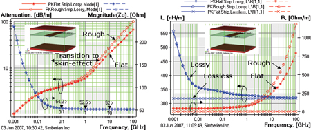
FIGURE 7. Attenuation PUL and characteristic impedance (left graph) and inductance and resistance PUL (right graph) of a 79 µ wide and 5 µm thick strip line (packaging example).
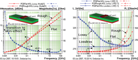
The first example is a 7-mil wide and 1.6-mil thick microstrip line with a dielectric substrate 4-mils thick and a lossless dielectric with relative permittivity4. Plane thickness is 2 mils. According to our classification, the medium frequency range for such a line is from 0.66 MHz to 66 MHz. (Strip thickness ranges from 0.5 to 5 skin depths.) The results of the transmission line parameters extraction from 1 MHz to 100 GHz (five decades) are shown in Figure 6. The effects of the transition to skin-effect, skin-effect, roughness and high-frequency dispersion can be observed on the graphs.
The second example is a 79-µm wide and 5-µm thick strip in a lossless homogeneous dielectric with Dk = 3.4. Distance to the top plane is 60 µm and to the bottom plane is 138 µm. Top plane thickness is 10 µm, and the bottom plane thickness is 15 µm. The extraction results are shown in Figure 7. This example was taken from reference6. However, dielectric losses are not accounted for here to distinguish from the conductor-related effects. Note that the conductor surface rms roughness in this example was different for the opposite surfaces of the strip as shown in Figure 6. The transition to skin effect in this example takes place at frequencies from 43 MHz to 4.3 GHz, which is clearly visible on the attenuation graph for instance.
In both examples, we neglected dielectric losses and dispersion related to polarization. The extraction results would be different if the dielectric loss and dispersion were taken into account. If a static solver is used for the first PCB example and loss parameters extracted at 1 GHz, the results of the analysis would be comparable with the full-wave analysis for frequencies around 1 GHz and if conductors are not rough. Though static solvers would fail to predict the behavior of the packaging interconnect because of the loss extraction frequency, 1 GHz is in the middle of the transition to skin-effect.
The only limitation of the used extraction technology is that it does not capture the first transition from DC to the state with current concentrated below the strip at a low frequency band.
Conclusion
Considering the conductor effects discussed in this paper, a wish list of requirements for an ultra-broadband extraction tool for analysis of serial data interconnects can be compiled as follows:
- 3D full-wave analysis to extract parameters of transmission line and transitions.
- Simulate DC and low-frequency current crowding in planes.
- Simulate transition to skin-effect, shape and proximity effects at medium frequencies.
- Account for skin-effect, dispersion and edge effect at high frequencies.
- Have conductor models valid and causal over five to six frequency decades in general.
- Account for conductor surface roughness.
- Automatically extract S-parameters and frequency-dependent modal and RLGC matrix parameters per unit length for W-element models of multiconductor lines.
Though transmission line parameter extraction usually requires broadband and causal conductor models, via-hole analysis may be done with simplified models and sometimes even neglecting conductor loss. This is because of the relatively small electrical length of the via and the dominance of the reflection and radiation losses. There is no an ideal tool that suits all those requirements. Thus, tool selection for a particular problem requires an understanding of the limitations and benefits of the built-in in the simulator technology. Being 3D and full-wave does not mean the highest accuracy possible, and sometime even a 2D static field solver may provide more accurate solutions than a 3D full-wave solver without broadband conductor models. PCD&M
Yuriy Shlepnev is president of Simberian Inc. He can be reached at This email address is being protected from spambots. You need JavaScript enabled to view it..
REFERENCES
1. A. R. Djorjevic, T. K. Sarkar, Closed-form formulas for frequency-dependent resistance and inductance per unit length of microstrip and strip transmission lines, IEEE Trans. Microwave Theory Tech, vol. 42, N 2, 1994, p. 241-248.
2. J. Rautio, An Investigation of Microstrip Conductor Loss, IEEE MTT Magazine, December 2000, pp. 60 – 67.
3. A. Deutsch, C Surovic, R. Krabbenhoft, G. V. Kopcsay, B. Chamberlin, Losses caused by roughness of metallization in printed-circuit boards, - in Proc. of 14th Topical Meeting on Electrical Performance of Electronic Packaging, 2005, p. 39-42.
4. Y.O. Shlepnev, “Trefftz finite elements for electromagnetics”, – IEEE Trans. Microwave Theory Tech., vol. MTT-50, pp. 1328-1339, May, 2002.
5. Y.O. Shlepnev, "Trefftz finite elements for electromagnetics", - IEEE Trans. Microwave Theory Tech., vol. MTT-50, pp. 1328-1339, May, 2002.
6.Simbeor - 3D full-wave field solver for multilayered circuits, Simberian Inc., www.simberian.com.
7. A. Byers, “Accounting for high frequency transmission line loss effects in HFSS”, in Proc. Ansoft User Workshop, Los Angeles, CA, 2003
