Modeling Issues in High-Speed Simulation
High frequency digital signals require complex models to accurately simulate the signal’s path.
Until recently, designers performing high-speed PCB simulations worried mostly about finding IBIS models for driver and receiver ICs. By the late 1990s, models could easily be downloaded from vendor Web sites, although the quality of the models was a concern. Still, spurred by demands from a knowledgeable user community, IC vendors gradually became better at providing well-tested, ready-to-use IBIS models.
Recently, the complexities of higher-speed signaling have demanded additional types of models – for not only IC buffers, but also for packages, vias and connectors. This article surveys these new, and sometimes difficult, requirements.
Anatomy of a Signal Path
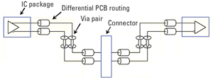
To understand the models required in a modern high-speed analysis, it’s helpful to look at a typical signal path channel. Figure 1 shows a worst-case path, with a pair of differential SERDES drivers/receivers and their packages; PCB interconnects, including vias near both ICs; and a connector mid-path. This is a daring design as it involves multi-gigabit signal transmission, yet risks passing the signal through two pairs of vias and a connector. Without detailed simulation, it’s not possible to say whether this channel will even function.
|
|
Signal integrity (SI) simulation has long relied on decomposition, in which a larger-scale analysis is broken down into a set of sub-pieces. Each piece is modeled in the best possible way and then re-assembled back into an appropriate simulator. Exactly the same approach can be used with the channel in Figure 1, except that when we decompose it, we’ll find requirements for new types of models not used in classic SI simulation. Breaking down the figure from left to right, we find the following elements:
- SERDES driver buffer (possibly with pre-emphasis)
- IC package
- PCB trace routing
- Via
- Connector
- SERDES receiver (with clock/data recovery and possibly equalization)
SERDES Drivers and Receivers
SERDES drivers/receivers are more difficult to model than traditional digital buffers for several reasons. The first is that SERDES signaling involves significantly higher frequencies than are used in lower-speed technologies. This places more stress on a model and requires higher accuracy. For example, while traditional IBIS allows one lumped capacitance for a driver output, in reality these capacitances are formed in a more complex way and may vary in time or with output voltage. In a higher-speed simulation where a few tens of picoseconds may make a significant difference in a timing-margin calculation, this more detailed modeling may be required.
Additionally, SERDES drivers/receivers rarely involve only a simple analog buffer stage. Drivers often include pre-emphasis circuitry, and receivers may include large amounts of additional circuitry to implement clock-data recovery (CDR) and analog or digital equalization. IBIS models can handle little of this important functionality.
Does this mean that IBIS modeling is dead in the near future? Not at all. A basic principle of modeling is to always use the simplest, fastest model that has sufficient accuracy. Overkilling a model may seem like an always-safe approach, but it’s unwise. More complex models are usually difficult to obtain and understand, and are always much slower running than a simpler alternative. Also, the IBIS Open Forum, aware of the need for more detailed modeling, has allowed IBIS to “wrap” models expressed in other, more flexible languages such as SPICE or AMS. Plus, many high-speed interfaces (like DDR2) have continued to be served well by pure IBIS models.
Many users assume that SPICE is the natural follow-on to IBIS, especially for SERDES. SPICE does indeed have at least one important advantage: Because it models buffers at the transistor level, it provides an ultimate level of accuracy. But SPICE also has drawbacks. First, SPICE models contain so much detail that IC vendors invariably demand encryption, which makes the model harder to work with. Also, encryption is simulator-specific, limiting users’ tool choices. Second, SPICE models are less stable than other types. Users often have to worry about convergence problems. For digital designers not experts in SPICE, this can be a major barrier.
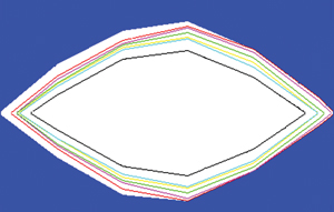
Third, and most significant, SPICE models are simply too slow for some applications, especially for SERDES signaling. When data rates reach the point where interconnect delays are longer than bit periods, intersymbol interference (ISI) effects become important and many long, bit eye diagram simulations are required. In fact, to validly simulate a SERDES link requires millions or even billions of bits, an impossibility with SPICE. Each order of magnitude increase in stimulus length closes the eye diagram more, as shown in Figure 2. A simulation based on only 10,000 bits (already a strain for SPICE) is essentially worthless.
|
|
Options for SERDES Modeling
Fortunately, there are modeling options between IBIS and SPICE. One intriguing possibility is the AMS languages (VHDL-AMS and Verilog-AMS), which add analog/mixed-signal capability to the digital versions of these standards. AMS models have several potential advantages. First, models of almost arbitrary complexity can be described, overcoming the accuracy limitations of IBIS. Second, AMS models can be described at a behavioral level, which obviates two of SPICE’s limitations: slow simulation and lack of IP protection. Another important advantage of AMS modeling is that it supports a mixture of analog and digital behavior, allowing circuitry for pre-emphasis, CDR and equalization to be described. AMS models can even be “taught” how to be self-measuring, so that they can automatically extract timing data and check for SI violations.
Unfortunately, VHDL/Verilog-AMS is not a panacea. For example, even though the performance gains vs. SPICE are at least three orders of magnitude, AMS models still can’t practically produce eye diagrams with more than approximately 10 million bits. Also, many of the silicon-vendor engineers responsible for creating models aren’t familiar with AMS languages. Finally, not all EDA vendors are able to support AMS in their high-speed tools.
Another emerging possibility is currently being discussed by the IBIS Open Forum: allowing semiconductor vendors to provide “black-box” executable models that could exchange data with SI tools. Advantages would be flexibility for model creators (models could be written in any language), execution speed and thorough IP protection. The challenge would be to support each SERDES vendor’s unique requirements for data exchange in an interoperable manner. However, not enough is known about the viability of this option at press time to merit more detail.
One final technology that may have a strong positive impact on SERDES modeling is the ability to predict the stimulus sequence that will produce worst-case simulations, based on the characteristics of the channel and attached IC buffers. Normally, designers seek worst-case results by simulating with extremely long, random sequences. Using this technology instead, a much shorter worst-case sequence can be predicted and random stimulus avoided. Such sequences are often only several thousand bits in length, and potentially make simulation with any kind of IC model fast enough.
IC Packages
As if modeling IC buffers weren’t complex enough, another major consideration with high-frequency signals is the package that houses the ICs. At lower frequencies, it was sufficient to model them with a simple per-pin L/C/R circuit. Unfortunately, this is no longer accurate enough. Now crosstalk and, generally, more frequency-dependent electromagnetic detail, is required.
Good-quality models of IC packages are not easily generated. Models must be created either by measurement or electromagnetic (EM) extraction. Usually 3D EM tools are used; their native output is S-parameter models, in Touchstone format. Only rarely would users of SI tools create such models themselves, for at least two reasons:
- 3D extraction tools are difficult to use and require expert manipulation to yield good results.
- Usually only the manufacturer has access to the geometric and materials detail of the package’s construction.
S (and Y or Z) parameters are frequency-domain models, consisting of tables at a large number of frequencies describing the energy transmission between designated “ports” on the model. Yet in most cases, users want to simulate with them in the time domain. Thus, an important tool-related issue is how a given circuit simulator handles frequency-domain models in the time domain. Nearly all circuit simulators can accept S-parameter models, but potential problems abound when simulations are actually run. Large models often fail to simulate, or simulate slowly. Causality and passivity errors in the models are passed, uncorrected, directly into simulation results. Accuracy can also be compromised in algorithmic attempts to keep performance acceptable.
To avoid these limitations, some users convert S-parameters into equivalent circuits. SPICE-based simulators generally handle circuit networks better than large S-parameter models, but this workaround has problems. One problem is that the resulting circuits are usually very large and simulate slowly. Another is that the solution of circuit networks over time accumulates error (an effect known as “local truncation error,” or LTE). In short simulations this is not a concern, but in long-simulations it can be a source of major inaccuracy. Perhaps worse, LTE, as well as causality and passivity violations, are invisible – the user sees normal-looking waveforms and trusts them, when they’re actually hiding subtle but very real simulation inaccuracies.
PCB Traces
Of all aspects of channel modeling, the one that it is most mature models for PCB traces. Traces on a well-designed PCB can be modeled as coupled, lossy transmission lines known as t-lines. T-line technology has been the heart of SI simulation for two decades, and by the late 1990s, most simulators had strong support for it, including advanced loss effects. Of particular concern is loss modeling where the potential difficulty is in reproducing lossy effects, in both metal and dielectric, over a very wide range of frequencies.
A point that is often missed when comparing SI and electromagnetic tools is that the EM tools typically come from the RF- and microwave-engineering worlds where extremely high-frequency effects are only considered over a narrow range of frequencies. Analysis of digital signals, on the other hand, requires accurate modeling over many decades of frequency, spanning from high harmonics of the fundamental bit rate down to low frequencies.
Vias
Other potentially serious obstacles in a high-speed signal’s path, once they exit the driver-IC package and begin navigating the PCB, are vias. In fact, some designers of SERDES channels try to avoid vias entirely, a strategy that comes from RF/microwave design. Unfortunately, the densities of modern digital PCBs – especially as routing tries to break out of a BGA package with 1,000+ pins – is such that vias are unavoidable.
Electrically, vias represent a major vertical discontinuity to the signal path. Implicitly, the assumption in a PCB signal path is that the signal flows cleanly on a given stackup layer, with one or two reference layers in which the signal’s return current can flow uninterrupted. But vias violate this assumption, making their return-current behavior suspicious, unless carefully designed. A via can easily generate the following interrelated problems: impedance mismatch and signal reflection, crosstalk with other vias, and substantial noise generation between plane layers.
|
|
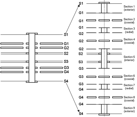
Good SI tools now model a via by decomposing it into sections, and calculating L and C values for each, as shown in Figure 3. But at high frequencies, even this type of decomposition is often insufficient because not enough detail is included about the via’s return-current mechanism.
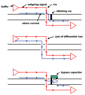
To completely predict a via’s behavior, it is often necessary to consider the surrounding structures on the PCB, i.e., those elements that determine how the return current for the via’s signal forms. An important distinction must be made between vias that are localized (designed to be self-sufficient in terms of return current), and those that are not and rely on “accidental” structures all over the PCB to carry return current. Figure 4 shows several examples of localized vias.
|
|
The via + stitching and the differential via pair are designed to carry their own return current, so they tend to be well behaved. The via with bypass capacitor forms a localized return path only at some frequencies; at others, it behaves like a single-ended via with return currents spread all over the PCB. Non-localized vias can only be analyzed using special EM simulators capable of efficiently entire boards.
Capacitors
The previous section mentions the role of capacitors in forming return currents. If return currents are to be modeled, then capacitors must be, as well. But what constitutes a detailed enough model for a bypass/decoupling capacitor?
Obviously, step one is to know the capacitor’s value. This is not as trivial as it sounds because the tolerance on many capacitors’ values is often as bad as 20%. Next to consider is the parasitic inductance of the capacitor, which depends mostly on how the capacitor is mounted to the PCB’s plane layers. This inductance is what determines the capacitor’s impedance profile.
The bottom point of a capacitor’s impedance curve is determined by its effective series resistance (ESR). To first order then, the capacitor’s circuit model is a series combination of C, ESR and self + mounting inductance. However, at higher frequencies even this model is too simplistic, so vendors of high-speed capacitors typically offer S-parameter models.
Connectors
Vias are not the only major discontinuity in Figure 1’s signal path. Unfortunately, this design also contains a connector. Some designers are lucky; their projects involve only a single board. But a recent survey found that 70% of designs involve two or more interconnected PCBs. In some respects, connectors are similar to vias: they both represent potentially big signal discontinuities, and in both, the handling of return currents plays a major role in determining how well they pass high-speed signals. The difference comes mainly in the freedom an engineer has to design a solution; vias are typically designed from scratch, whereas connectors are designed by a third-party vendor and the engineer chooses between several pre-built solutions.
The key to making a successful connector choice is a high-quality model for simulation. Here, the user is dependent on the connector vendor. While it’s possible to measure a connector’s behavior using a vector network analyzer (VNA), such measurements are difficult to make accurately at high frequencies and are best left to experts. Many connector models are actually not measured at all. Instead, a detailed 3D model is constructed and EM extraction software is applied.
Unfortunately, neither approach is foolproof. A major issue for users of connector models is determining their quality, and if necessary, fixing them. Thus, useful simulation tools must include not only the ability to simulate with such models, but also the ability to check their quality. Problems with causality and passivity must especially be avoided.
As digital signaling moves to higher and higher frequencies, more types of increasingly complex models are needed to accurately simulate a signal’s path. Users need to be sure that their analysis tools are capable of handling as many of these models types as possible. PCD&M
Steve Kaufer is director of engineering for High-Speed Tools at Mentor Graphics Corp. He can be reached at This email address is being protected from spambots. You need JavaScript enabled to view it..


