Vertical Integration – The Old Model Still Proves a Successful Strategy
Economies of scale, cost reduction, product differentiation and supply chain control are key drivers for vertical integration strategies.
Vertical integration became a well-known way to structure businesses in the post-war 1950s. Many value chain systems were adapted to suit a variety of industries. Most often supply chain control followed forward integration. In the post-war economy, control of raw material supply to prevent shortages was often more critical that the potential cost savings afforded by the integration prospects.
Nan Ya Plastics Corp. was founded in 1958, with businesses in processed plastics, DOP, stabilizer, polyester fiber and other integrated activities. In the 1980s the electronics business in Taiwan began rapid development. In reaction to the opportunity Nan Ya Plastics expanded to develop an Electronics Materials Division. Started in 1984, the initial projects included copper clad laminate, epoxy resin, glass fabric and copper foil investigations. The plan from the beginning was to include vertical integration of raw materials critical to the developing personal computer and printed circuit board industries.
|
|
Nan Ya’s copper clad laminate (CCL) division has multiple facilities in Taiwan and has recently expanded to include an additional campus in northern China. The operations in Taiwan consist of multiplant locations with individual specializations. Epoxy resin manufacturing is located in north and southwest Taiwan, glass yarn production in the north, glass cloth fabrication in the southwest, copper foil manufacturing in the southeast and copper clad laminate production in both north and southwest locations in Taiwan.
In Kunshan, China all manufacturing occurs on the one square kilometer campus, that houses raw material generation, CCL manufacturing operations and PCB fabrication facilities. After only a few minutes on the Kunshan campus, it was easy to understand why the facility is often referered to as Nan Ya City. The single campus operation at Kunshan showcases the benefits of vertical integration that include reduced transportation costs, improved supply chain coordination, product differentiation through control of raw material input, enhanced margin position and the potential to expand into additional core competency areas.
Integration and Education
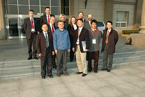
I had the privilege to be invited to the Kunshan facility earlier this year. My small group was joined by a larger delegation from Europe, sponsored by the EIPC. The EIPC delegates included Michael Weinhold from EIPC, who was kind enough to photograph the tour and has provided the pictures for this article; Ivan Ho of Cimnet; Dominique Pellizzari of Groupe Cire; Andreas Folge of Technolam; Takahashi Okudera of Yamamoto Mfg.; Rex Rozario and David Pike of Graphic Plc; Giovanni Tridenti of Somacis; and Wendy Heyes and Tom Parker of CC Electronics Europe (pictured in Photo 2).
|
|
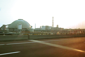
Following the highway to the campus entrance we crossed a river and then followed a large group of pipes along the parameter of the site. Raw materials, coal, silica and resin precursors like Bisphenol-A arrive at the Nan Ya site by boat and are piped or transported by rail to the appropriate buildings.
Nan Ya begins its vertical integration at the very beginning. In a power plant at the edge of the campus, Nan Ya makes its own electricity, taking vertical integration a step further towards a totally self-contained and controlled environment. There is good reason for this move. The campus uses a high level of power. The copper foil manufacturing area in particular consumes 50% of the power currently produced on-site to run the 42 copper foil producing electroplating lines.
Kunshan is the smaller of Nan Ya operations, with about 7,000 employees. There are over 15,000 people in the Taiwan facilities. The Kunshan facility is approaching 50% capacity. The site footprint calls for three phases, allowing for ramp up and expansion of all operations. Some operations are still in phase one (CCL and copper foil) and others are moving into phase two (PCB fabrication), so additional space and buildings exist to increase output by more than 50% in the future.
The majority of the people who live onsite in the company dormitories work in the PCB fabrication facilities. Over 50% of the people on the Kunshan site work in PCB manufacturing. Only about 10% work in CCL manufacturing. The remainder of the employees support facilities operations including the power plant, transportation and waste/water management systems. The CCL manufacturing process has the highest level of automation, reducing the need for operators dramatically.
Like many companies in China today, Nan Ya has problems with worker turnover. Many workers come to Nan Ya for the world class PCB manufacturing experience they can gain there and leave after 12 to 18 months to work for smaller companies where the experience gained at Nan Ya increases their value.
The vice general manager, H. C. Yama Yen said that Nan Ya is considered the premier “PCB University” in China. Going hand in hand with their excellent worker training programs comes an inherently higher risk of employee turnover.
The problem of high turnover is not specific to Nan Ya. In 2005, China had an average turnover rate of 14%, up 8% over 2000. This is compared to 3% turnover rate for 2005 in the United States that has remained relatively constant. In China the areas close to big cities are particularly susceptible, with turnover rates often over 25%. Factory workers have the shortest tenure, exhibiting the highest rate of turnover.
“Job hopping” in China is a problem that most companies need to deal with. Nan Ya’s approach has been to incorporate continuous training for all of their employees to assure that their workers, whether newly hired or long time employees, know how to do their job well.
Tour of Raw Materials Manufacturing
The overall Nan Ya CCL facility consists of glass yarn and glass fabric manufacturing, copper foil generation, epoxy synthesis, and the CCL treaters and lamination facility.
We began with glass fabric weaving. Glass yarn enters into the fabric weaving area where looms weave fiberglass cloth in 7628 and 1080 style glass thicknesses. Each of the glass fabric plants is designed to produce 6.5 million meters of fabric a month. Fabric manufacturing is in phase two, with an estimated output of 16 million meters per month. The room we walked through had 500 textile looms, weaving glass yarn into fiberglass to the rhythmic clatter of the shuttles. Not what I had expected to see at the start of the copper clad laminate facility tour, and therefore all the more impressive.
From fabric weaving we traveled across the road to the copper foil manufacturing plant. Here 42 specialized electroplating machines deposit 1,400 metric tons of copper foil per month. As previously mentioned the copper foil manufacturing operation consumes quite a lot of power, about 50% of the Kunshan power plant output. Like most of the manufacturing areas on CCL campus, this production process runs around the clock with minimal support personnel.
Right along side of the copper foil manufacturing operation is epoxy synthesis. Nan Ya reacts its own epoxy materials. It currently offers a wide range of epoxy types including high Tg materials and halogen-free laminates. About 30% of the laminate produced in Kunshan is high Tg laminate, 65% is traditional FR-4 and 5% is special products including a growing output of halogen-free material. Epoxy output exceeds 135,000 metric tons per year.
The Copper Clad Laminate Facilities
Nan Ya’s approach to CCL manufacturing is quite similar to other laminate companies. Glass fabric is received into the manufacturing area after desizing and finishing still on jumbo rolls. The laminate varnish, a mixture of a specific epoxy base, along with an accelerator, hardener and solvent is blended for the treater run. Glass fabric is loaded into the treater and coated with resin and cured in the treater tower. B-staged prepreg is then cut for use in laminate manufacturing. Plant 1 runs 20 treater towers.
The lamination process involves the layup of Nan Ya-made prepreg and copper foil that is then pressed in large lamination presses. Nan Ya uses double wide lamination platens, producing a laminate sheet that is twice the size of standard 36? x 48? sheet. Output from the automated 36 opening presses is 1 million jumbo sheets per month.
Focus on Technology and the Environment
The visit to the Nan Ya Kunshan campus was awe-inspiring. The size and scope of the campus was only part of the reason. As we moved from operation to operation, there was consistent appearance of order and cleanliness. Clean room environments dominated many of the manufacturing area. A high level of organization and a rational product flow made sure that raw materials moved from place to place when needed.
The facilities for waste treatment were extensive. Ninety percent of the waste water generated by the copper foil manufacturing plant is reused. The remaining 10% is concentrated by evaporation methods and reused in the manufacturing operation. The Electronics Division goal is zero discharge. Specific care is given to air quality, with elaborate treater solvent recycling systems that process waste air from treater ovens through activated carbon before it is release to the atmosphere.
The corporation continues to push for technology improvements, including halogen-free laminate and IC substrate materials, low Dk materials, low CTE materials and a number of specialized products for build-up technologies including resin coated copper foil and film type build-up materials like specially developed laser ablatable prepreg.
A View to the Future
It’s interesting to note that discussions about vertical integration are slowing working their way back into the electronics industry after the long hiatus spurred by OEM cost cutting measures. The approach, however, that Nan Ya expounds is not the same as what is surfacing in the EMS world1. It was conceived when vertical integration was king and has been honed to perfection over the past 49 years.
In an economic climate that needs to deal with rising commodity product costs such as oil and metals, and potential raw material shortages due to expanding markets, the idea of controlling one’s entire raw materials supply chain and the associated cost, is very attractive. Unfortunately not many PCB companies in the world can proceed to vertically integrate to the extent that Nan Ya has done.
Nan Ya plans to continue expansion and further upgrade product technology. There has been a steady shift towards higher Tg and halogen-free laminate materials since 2006 and the introduction of RoHS in Europe. Nan Ya currently manufactures only PCB materials in the Kunshan plant. All substrate laminates and resin coated copper foil are manufactured in Taiwan.
The long-term goal is for the Kunshan campus to be fully operational. Once all phases are complete, the output volume will surpass that of the Taiwan operations. Based on the experience gained in Taiwan, Nan Ya has had the opportunity to plan the Kunshan facility in a single location. The campus has been build to suit the requirements of a vertically integrated CCL and PCB manufacturing environment.
Prospects are good that Nan Ya will continue to capitalize on the economics of scale gained by the vertical integration model. Nan Ya was ranked seventh in the NTI Top 1002 for 2005 after turning in a $250 million increase over 2004. The Kunshan campus provides a location for focused PCB activites while Taiwan concentrates on expanding the IC substrate business. With the flexibility that the Kunshan campus provides for focused PCB activities, allowing the Taiwan locations to concentrate on developing the IC substrate business, it’s easy to predict a rapid ascent to the top spot for the company. PCD&M
Kathy Nargi-Toth is editor of PCD&M.
REFERENCES
1. Return of the One-Stop Shop, Buetow, M., Circuits Assembly, May 2007.
2. The Big Get Bigger, Nakahara, H., Printed Circuit Design & Manufacture, September 2006.


