10+ Gb/second Signal Considerations
Improving layout technique and focusing on physical layer structure can optimize signal integrity.
With today’s high-speed chipsets transmitting data above 10+Gb/s, and rise times going below 30 ps, even small parasitic inductances and capacitances can degrade a signal and introduce noise. Occasionally, PCB layout is regarded as one of the last steps in the design process. However, it happens to be the most critical aspect at speeds where even the slightest discontinuities can cause signal integrity problems.
The introduction of many high-speed digital standards, such as Serdes, PCI Express, SATA, Firewire and others, have pushed the performance limit to the maximum. The proliferation of serial links beyond 10 Gb/s has introduced signal integrity problems that expose poor design techniques of any physical component layer of the system. It could be the cable that runs the high-speed signal, the connectors or the strip-line/micro-strip on the PCB.
Coaxial cables are used in high-speed applications because they can ensure little signal degradation. The cable works well to control signal propagation speed, reduce crosstalk, lower noise pick up and provide an excellent impedance match at high frequencies.
When the signal is launched from the cable to the PCB, interconnections may cause problems at high speeds because of impedance discontinuities that exist between the cable, connector or the board. At 10+Gb/s speeds, even the slightest changes in geometries may cause discontinuities. The signal will reflect and result in degradation of signal integrity.
Specialized connectors are used with proper shielding. A well-designed connector integrates mechanical, chemical and electrical properties of the device seamlessly. Special modeling, simulation and measurement validation are required to ensure smooth transition of the signal from the cable to the trace.
Once this transition has been taken care of and the signal is safely on the PCB, it becomes the responsibility of the layout designer to ensure its signal integrity. In general, SI problems fall into four areas:
EMI
If a current travels through a trace or wire changes, it can create a changing electromagnetic field. By the laws of electromagnetic induction, this can induce a similar current in an adjacent wire. The induced current is directly proportional to the rate of change of the field in the active line. Faster rise times mean that the current is changing faster. Hence, EMI can create grave problems in high-speed applications such as:
- The design may fail FCC compliance testing.
- The design may be sensitive to temperature or voltage variations.
- The design may be sensitive to slight variations in fabrication.
- The design may not work reliably.
To find the solution to these problems, the cause must be studied. It’s known that current in a circuit flows in a closed loop and is the same everywhere. So if the signal current generates EMI, the return signal also creates an EMI that is similar in magnitude and opposite in direction. If the signal and its return are close enough, the radiation generated by both cancels each other. Hence, in order to reduce EMI, the loop area has to be minimized.
High-speed (AC) signals tend to return on the lowest impedance path. Therefore, a plane underneath the trace would be an obvious choice for them. A micro-strip structure would work well from an EMI standpoint. These high-speed traces should be routed over their reference plane. If they are allowed to cross splits or slots it can create a larger loop area since the return has to move around the slot.
EMI is difficult to control if proper provisions are not made for a signal return through a connector. Therefore, pin assignment in these devices and connectors is very important. Each high-speed signal pin should have a ground pin nearby for the signal to return. This reduces the loop area and reduces EMI.
Another way to control EMI on the PCB is to avoid stubs. Any un-terminated trace that is left hanging can be a stub and, depending upon the rise time of the signal, can act as an antenna. Such antennas are never beneficial and should be avoided.
Common mode (CM) currents are another cause of EMI problems that are hard to pin point. CM currents are currents that flow in a circuit along a path other than intended. A strip-line environment is the best way to minimize these currents to control EMI for high-speed signals.
Reflection
Consider a long straight wire carrying a signal, with its return nearby. The wire has some inductance associated with it and there is some capacitance in its return. Figure 1 shows such a wire with its infinitely long network of capacitors and inductors. This is a transmission line model.
|
|
A driver sends such a signal down a transmission line. If the load does not absorb the entire signal, some of it reflects back to the driver and may cause ringing at the load receiver. This reduces the dynamic range of the receiver and may cause false triggering. If the signal’s rise time is shorter than the propagation time of the signal and back again, this can cause the signal to reflect. Hence, most of the high-speed signals should be treated as transmission lines. To avoid reflections, these signals have to be properly terminated.
A transmission line terminated at its characteristic impedance Z0 looks like an infinitely long transmission line. Here the signal is completely absorbed by the trace and receiver, and does not reflect. When the impedance of the source Zs is equal to the impedance of the trace ZN as well as the load impedance ZL, the result is a perfectly terminated transmission line.
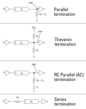
There are several methods of termination (Figure 2), each with pros and cons:
|
|
Parallel termination. A termination resistor RT that is equal to the line impedance Z0 is placed close to the load. This type of termination works well with distributed loads but has a higher power requirement since some power is dissipated in the resistor.
Thevenin termination. A pair of termination resistors is used near each load. These resistors can also perform a pull up, pull down function and improve noise margins. However, the actual values of R1 and R2 are difficult to calculate. They also act like a switching gate and may require decoupling capacitors to be placed nearby to reduce EMI.
RC Parallel (AC) termination. A capacitor is added in series to the terminating resistor in this type of termination. RT = Z0, and the capacitor blocks DC current so there is no DC power drain. The capacitor’s value, however, is difficult to calculate. A larger capacitor will delay the signal due to slower switching, and using a very small capacitor may reduce its effectiveness and even cause the signal to overshoot.
Series termination. Series termination offers a good low power solution. A series resistor is used and placed near the driver instead of the receiver. The signal that reflects back is absorbed by this resistor before getting to the driver. The driver’s impedance plus the resistor equals the trace impedance.
At very high speeds, the rise time degrades because of increased RC time constant. At these speeds, a pre-layout signal integrity simulation with input output buffer information specification (IBIS) must be done before using this termination scheme.
Crosstalk
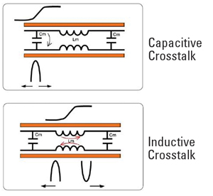
As the system performance and board densities increase, the problem of crosstalk and how to deal with it become more important. Crosstalk is the transfer of energy between adjacent conductors due to mutual inductance and shunt capacitance. The coupled energy from the active line is superimposed on the victim line. The coupled signals that flow towards the receiver constitutes forward crosstalk. Those traveling towards the source constitute backward crosstalk. Backward crosstalk is the sum of the inductive and capacitive coupling, whereas forward is the difference between the two (Figure 3).
|
|
Crosstalk is a major issue in high-speed designs because it is directly proportional to the edge rates of the active line. Other factors are the proximity of the two lines and the distance over which the two lines run parallel to each other. Hence, the high-speed signals should be routed as far apart as possible. Ideally, the distance from center to center should at least be four times the trace width for these signals.
The distance that the line runs parallel to each other should also be kept to a minimum. Other solutions include reducing the dielectric spacing between the line and its reference plane or introducing a co-planar structure, where a ground plane is inserted between the traces. Terminating the line on its characteristic impedance can also reduce the crosstalk by as much as 50%.
Power System Stability
The purpose of a decoupling system is to provide a low impedance power system on the board as well as meeting every device’s switching needs. The devices that transmit data at 10 Gb/s and over have special decoupling and layout requirements. If the rise time is short, a significant voltage drop can occur across the inductance path between the power supply and devices. Moreover, if a high pin count BGA is used, there can be substantial amount of transient current that flows through this path. This may cause a wide range of problems, from slowing down the propagation time to false triggering.
Usually, there are two approaches employed – traditional and power system impedance. In the traditional approach, decoupling capacitors are placed between the device and the stray inductance that can contribute to ground bounce. Usually the larger one is used for bulk charge and the smaller ones for a faster response that provide the switching requirements. That is why the smaller caps are placed closest to the chip. Power and ground planes can also be used to provide the small, but very fast planar capacitance. Here the small distance between adjacent power and ground plane provides the capacitance.
As for the power system impedance approach, the entire PCB is viewed to try to get a target impedance of the power system at all relevant frequencies. When the whole system is taken into account, an impedance is created that is high at DC, but low at all other frequencies. In this area capacitor placement is not as important as the choice of the capacitor itself. There should be a wide range of values and self-resonant frequencies that have moderate equivalent series resistance (ESR). Planar capacitance is a must here.
New, faster designs call for a combination of the two approaches. The power system approach is applied and then assurances are made that there is substantial decoupling at each power pin of the device to provide its switching requirements.
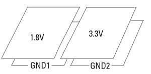
In high-speed layouts, designing multiple planes and dealing with split planes are a very important part of creating a stable power system for a PCB. Every high-speed trace should be referenced to a continuous plane. If these traces are allowed to cross splits, it may cause the three problems of impedance mismatch, EMI and crosstalk discussed earlier. Unrelated planes should not be allowed to cross each other on adjacent layers (Figure 4). Planes belonging to different logic families, if allowed to overlap, can cause capacitive coupling between the two planes, which is an EMI problem.
|
|
As the telecommunications industry gears towards high-speed data transmission, digital designers must push the performance limit of what is possible to achieve on copper. Faster rise times can expose poor layout techniques, with problems ranging from the design being sensitive to power supply variations to the final design that is intermittent in the field. Optimizing signal integrity by focusing on each physical layer structure can produce astonishing results. If the techniques that are described in this article are followed, problems like ringing, EMI and crosstalk can be reduced to a great extent, if not eliminated. PCD&M
Syed W. Ali (This email address is being protected from spambots. You need JavaScript enabled to view it.) is a certified interconnect designer and layout engineer at Nexlogic Technologies Inc.


