Designing for High Layer Count
The design team plays a major role in reducing emissions, increasing immunity and improving signal quality for complex, high-speed PCBs.
Today’s PCB is not just a plain electrical interconnection device. It is a multifarious, highly specified component in its own right. It brings an increased requirement for board design verification prior to manufacture. Ever-increasing speeds and complexity of modern circuitry demand high quality controlled PCB impedance and EMC. Above 25 MHz, multilayer boards should be considered because of several key advantages they provide, including: significant radiated emission reduction compared to two layer PCBs; decreased ground impedance, which leads to decreased ground noise; and the allowance of signals to be routed in a microstrip or stripline configuration. These configurations are controlled impedance transmission lines with lower radiation than random traces used on a two-layer board.
Choosing and designing the most effective layer stackup for a PCB design is a key stage during early product development. By selecting the most appropriate stackup, a PCB design can be optimized for cost, signal integrity, thermal performance and reliability. Four factors are important with respect to board stackup considerations.
At layer count, it’s important to consider via effects, thermal performance and EMC. Secondly, power and/or ground planes, the number of them, and noise and return paths need to be checked. Next, the designer must review layer sequence to include symmetrical and asymmetrical layer stackup. Lastly, spacing between layers must be considered to include embedded capacitance and impedance control.
In deciding on the number of layers, net density needs to be considered. This involves the number of signals to be routed and associated cost that is incurred as a result of increasing the layer count. But factors such as signal frequency, environment (shielded or unshielded enclosure) and PCB requirements, such as Class A or Class B emission requirements, are usually ignored. But actually, at higher frequencies, these factors are as critical as the PCB’s density and cost.
Via Effects. Vias have a significant effect on high layer count boards, especially at high speed, whereas they have little impact at low frequencies. There are a number of negative via effects. Vias are inherently capacitive and can change signal characteristics. A trace can move from one layer to another and it can reference to a different reference plane that causes severe distortion in the trace’s characteristic impedance. A via causes reflection by a step function; it changes in the trace impedance.
A via’s adverse effects on signal integrity can be minimized several ways. The simplest method is to route critical traces with the least number of vias. Non-functional inner layer pads should be removed. Plus, using a microvia, buried via and controlled impedance via can minimize the damaging effects on signal integrity.
EMC. PCB stackup is a major factor in determining a product’s EMC performance. A poor stackup increases radiation from the loops on the PCB, whereas radiations can be reduced effectively by efficient stackup. In high layer count, significant radiation amounts can be controlled by using a number of ground and/or power planes that allow signals to be routed in the stripline or microstrip configuration.
In high layer count boards, the signal layer should be tightly coupled to its adjacent planes. High-speed traces should be routed on buried layers located between planes. Power and ground planes should be tightly coupled together. Multiple ground layers in high layer count PCBs are very functional since the internal ground plane that makes microstrip and stripline configurations possible also provides inherent shielding and isolation of signal layers. And the ground impedance can decrease, causing ground noise.
Types and Number of Planes. The role and sequence of planes play a pivotal role to assure multiple layer objectives are fulfilled. First, a signal layer should always be adjacent to a plane and tightly coupled to their adjacent planes in order to provide proper return path. Second, power and ground planes should be closely coupled to achieve buried capacitance. Third, high-speed signals should be routed on buried layers located between planes. In this way, the planes can act as shields and contain the radiation from the high-speed traces. Finally, multiple ground planes are highly advantageous, since they reduce board ground (reference plane) impedance and reduce common-mode radiation.
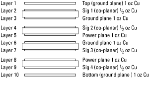
Satisfying all the objectives cited above with the right stackup means that a PCB is EMC compliant. All objectives can be achieved when a minimum of eight-layer stackup is used, however, a four- to six-layer stackup does not allow all these objectives to be met simultaneously. Figure 1 shows a suggested stackup that satisfies all the objectives described above.
|
|
Sequence of the Layers. From a mechanical point of view, another desirable objective is to have the PCB’s cross-section symmetrical (or balanced) to prevent warping. For example, on an eight-layer board, if layer two is a plane then layer seven should also be a plane. Because high layer count boards have significant thermal mass, the reflow equipment to safely reach peak temperatures is limited.
A board that warps while in use may cause a board to stop working correctly. Even a slight twist or bend in a board during manufacturing can make adding component devices difficult or may cause previously mounted electronics to break off. And that can cost manufacturers an inordinate amount of money. If the PCB is small, thin and densely populated with components, there is an invitation for warpage-related reliability problems.
Spacing Between Layers. Two objectives are achieved by controlling the space between the layers. One deals with embedded capacitance, the other, impedance. As for embedded capacitance, high-frequency noise on power supplies causes problems for nearly every digital device. Such noise is typically generated by ground bounce, radiating signals or even by the digital device itself.
The simplest method of curing power supply noise is to use capacitors to decouple the high-frequency noise to ground. Ideally, decoupling capacitors provide a low-impedance path to ground for the high-frequency noise, hence “cleaning” the power supply. The same result can be achieved by using embedded capacitance instead of standalone capacitors.
A very thin, double sided copper clad laminate (about 50 micrometers) is used as the internal layer of a multilayer PCB. This internal layer functions as an electrostatic capacity layer replacing the conventional bypass capacitor. The function of conventional bypass capacitors used in the board for an IC is shared by the overall area of the internal layer’s electrostatic capacity layer. No major change is required for the electrostatic capacitor layer since only special epoxy glass double-sided copper clad laminate FR-4 is used as an internal layer.
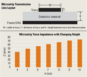
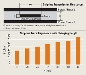
As for impedance, any PCB circuit trace has characteristic impedance associated with it. This impedance is dependent on trace width (W) and thickness (T), material dielectric constant (?r), and height (H) between the trace and reference plane. Impedance can be controlled by controlling these parameters.
|
|
|
|
Figure 2 (stripline) and Figure 3 (microstrip) show the effect on impedance by changing the spacing between the layers. Impedance mismatches produce the following detrimental effects in digital circuits:
- Digital signals are reflected between the input on the receiving device and the output on the transmitting device. The reflected signals are bounced back and forth between the two ends of the line until they are eventually absorbed by resistive losses.
- The reflected signals introduce ringing on the signal being sent across the trace. Ringing impacts the voltage level and timing of the signal, and can severely corrupt the trace.
- A mismatched signal path can cause the signal to be radiated into the environment.
If the proposed layer stackup guidelines in this article are followed, more reliable and efficient PCBs can be produced. Plus, many of the most common problems associated with high-speed dense boards can be avoided. These guidelines will assist in reducing emission, increase immunity and improve the signal quality of PCBs. To ensure that all these requirements are met, a design team’s expertise plays a major role to assure an optimum design is achieved in the minimum amount of time and at optimum cost. PCD&M
Faisal Ahmed and Ishtiaq Safdar are PCB layout engineers at NexLogic Technologies. They can be reached at This email address is being protected from spambots. You need JavaScript enabled to view it. and This email address is being protected from spambots. You need JavaScript enabled to view it., respectively.


