Organic and Printed Electronics: The Next Big Thing?
Printing processes promise high throughput at low costs.
The revolutionary concept of using graphic arts printing processes to manufacture electronic components such as wireless hardware (RFID), displays and ICs has been pursued since 2000 in corporate, government and university laboratories, and by well-financed startups. This manufacturing process is novel compared to traditional means used to produce these components (e.g., cleanroom environments and vacuum deposition); however, printing-like technologies are already used to manufacture PCBs. PCB manufacturing and graphic arts printing share similar heritage, as both are based on imaging, etching and engraving processes. Their convergence promises extremely high throughput at very low costs, and holds significant potential for flexible displays, lighting, sensors, RFID and smart packaging.
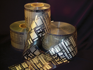
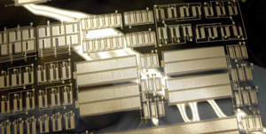
By taking advantage of new functional electronic inks (conductive, semiconductive and dielectric) and leveraging graphic arts printing platforms (gravure, flexography, inkjet), it is possible to reduce cost by several orders of magnitude and also significantly increase throughput over that of silicon IC manufacturing. Imagine, for example, printing all the electronics for a cellphone in a couple of hours via printing equipment typically used to pattern rich graphics posters and vibrant shampoo bottle labels (Figures 1a and 1b).
|
|
|
|
Together, organic and printed electronics is a disruptive technology that could affect a number of market segments without cannibalizing existing technologies. The technology has matured in recent years, migrating from lab to prototype production, and a supply chain is beginning to emerge.
The 2007 iNEMI Roadmap includes a chapter on organic and printed electronics to help define elements required for the technology’s successful commercialization. The Organic & Printed Electronics Technology Working Group (TWG), which produced this chapter, brought together 40 individuals, representing established businesses and startups in printing and electronics, to develop a “schematic†for the supply chain. The chapter they developed provides an overview of critical technologies for commercial launch and market diffusion of organic and printed electronics-based products. It addresses technologies specific to functional inks, substrates, packaging, printing platforms, characterization tools, design and modeling, and reliability. To the best of the authors’ knowledge, this roadmap is the first of its kind.
Functional inks. One driver behind organic and printed electronics is the development of new functional inks. Herein, the term “functional ink†refers to any solution-processable material. While graphic arts inks provide visual attributes, functional inks provide intrinsic bulk electrical, thermal, chemical or optical properties. During the past three years, significant R&D has gone into developing functional electronic inks (organic and inorganic) that can be printed on standard high-volume equipment common in the printing industry. Several families of functional inks (Table 1 [PDF format]
) have been commercialized recently or are under development with plans for commercialization in the next few years.
Development of various organic and nanoparticle synthesis technologies that provide inks suitable for high-speed print processes has led to the advent of a variety of functional inks. These conductive, semiconductive and dielectric inks have rheological properties that provide broad processing windows to enable low-cost manufacturing. Also, unlike previous functional inks, the new families are manufactured via robust synthesis and formulating routes, demonstrate greater stability in-air, and are ultra-compatible with large-area graphic arts manufacturing printing platforms.
In general, functional inks are grouped according to device application: 1) inks for passives such as membrane switches and touch screens, and 2) inks for actives such as ICs and LEDs. The 2007 iNEMI Roadmap identifies conductivity, mobility and dielectric constant as the critical attributes of functional inks. These capabilities are necessary to enable commercialization and market diffusion of printed electronics-based products. The roadmap also highlights the need for continued development of ink formulations with requisite rheological properties for different printing technologies.
Printing Platforms
As functional inks are developed, existing printing technologies are being enhanced to improve registration and produce finer printed feature resolution. Traditional printing technologies are classified into two categories: 1) contact printing, which includes letterpress, gravure, flexography, offset and screen printing, and 2) noncontact printing, such as micro-dispensing, jetting and “off contact†screen printing. Recently, efforts related to printed electronics have focused more on contact printing, primarily gravure, flexography, screen and offset, although inkjet printing has historically received the greatest attention.
Screen printing is commonly used for thick film deposition of conductors, resistors and capacitors. It is a preferred technology for membrane switch printing in which reliability and conductivity of the traces are achieved by printing a thick line of conductive material to withstand repeated impact strains. Screen printing’s resolution is generally coarser compared to other printing technologies. Recent applications have targeted RFID antenna fabrication, which requires electrically conductive and mechanically robust thick films.
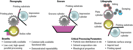
Flexography, a form of relief printing, lends itself to printing on nonporous materials, such as metal foils (Figure 2). Since flexography is a finer resolution printing technology, it is quickly gaining interest by RFID antenna printing suppliers as a manufacturing option that offers higher throughput than screen printing. Flexography requires a lower viscosity ink than screen printable inks, and yields printed dry films of less than 2.5 µm. Therefore, the flexography inks require higher bulk conductivity than those used in screen printing to compensate for the decrease in film thickness.
|
|
Gravure printing is quickly establishing itself as a viable manufacturing platform for printed electronics. Gravure platforms have the ability to print variable film thicknesses in one print unit (a feature that is limited in both lithography and flexography) and to provide both high resolution and throughput. These capabilities increase the potential of gravure for producing printed electronics. To date, superior resolution is achieved by the ultra-high image definition of the chromium-coated gravure cylinder, which has a hard surface that undergoes minimal distortion during the printing process.
Offset lithography printing, commonly referred to as “offset printing,†can also provide high-resolution printed features through precision control and balance of the plate surface energy for ink (imaging) and water/oil (masking) wetting. During high-volume printing, the printed dry film thickness approaches 1 µm with very tight tolerance.
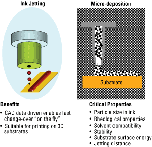
Inkjet printing is a noncontact printing technology that has been actively pursued for printed electronics during the past decade (Figure 3). The most attractive benefits of inkjet printing include digitally driven fabrication, on-the-fly product variability, additive processing and noncontact printing.
|
|
Despite their potential, today’s commercially available printing platforms are unable to provide the complete set of attributes necessary for printable electronics, and further development is required. The greatest challenges are registration and feature size/critical dimension. For example, reducing the electrical parasitic capacitance of the printed circuitry and achieving the highest circuit density for a multilayer circuit structure requires high tolerance registration. The need for high registration is further magnified when using flexible substrates, because they typically deform during imaging such that registration of subsequent layers may not be possible with predetermined parameters. This issue has led some to suggest that “active†registration and anisotropic distortion control may be required via vision and registration adjustment feedback hardware/software.
Concerning feature size and critical dimensions, traditional mass-printing techniques are mature and historically have not been challenged to reduce features below human vision resolution (100 µm). However, as interest grows in printed electronics, laser imaging of printing consumables (e.g., gravure cylinder engraving technologies, flexography plate fabrication processes) and inkjet are under active development, and feature sizes are expected to drop in the near future. In addition, ongoing efforts to improve printed electronics processing techniques and ink formulations will enable smaller feature sizes. For example, advanced polymer materials and novel nanoparticle technology have provided ink formulations with improved electrical performance while maintaining optimal rheological properties for printing (Figure 4).
|
|
Inline Characterization Tools
During the past 20 years, printing and prepress technology has evolved with the integration of electronic control systems, computer-aided architectures and digitization hardware. For example, programmable logic controllers and systems have replaced the hands-on manual controls of early printing systems to enable high-resolution rich graphics printing. As a result, the printing press has evolved from a craft-like machine to a high-volume manufacturing system with fully automated tracking of events that impact quality, such as inline splices, blanket washes, registration, inline color-control, ink metering and Web guidance. Although today’s advanced commercially available printing equipment has inline quality control hardware/software systems, successful transition of printed electronics from discrete testing of electronics offline to inline system testing during high-volume manufacturing will require the development of novel systems that leverage existing platforms from the microelectronics industry. Table 2 [PDF format]
lists several critical parameters to monitor during printed electronics manufacturing.
For organic and printed electronics-based products to benefit from economies-of-scale of printing platforms, manufacturing platforms with microelectronics-like inline characterization tools must be developed. Technical hurdles such as real-time quality control monitoring during production must be addressed. Attributes of printed electronics components and products such as device dimensions and electrical continuity require constant inline monitoring to ensure near 100% product yield during high-throughput printing.
The two greatest short-term needs for inline characterization tools are the design and integration of automated systems to monitor registration, coating thickness and defects at high resolution and at high manufacturing speeds (product pulse rates), and the development of hardware/software systems to enable the configuration of disparate printing technologies (e.g., press units). For example, a complex IC will need five or more passes through different print units that maintain high tolerance registration control, repeatability and substrate stability during transfer of the part between print units. Such complex electronics circuitry will be attainable after enhancement of existing print manufacturing platforms.
While there are no apparent showstoppers, the current technology gaps do present challenges. Table 2 [PDF format] lists several technology needs and potential solutions for inline characterization tools.
Inline characterization systems for printed electronics should draw from both print manufacturing and microelectronics manufacturing. Several systems have been identified by members of the printed electronics community that can be integrated into printing platforms: 1) a registration system that can automatically and simultaneously detect and correct both circumferential and lateral register errors, 2) an optical system that provides inspection and registration of up to 6,000 dpi (2 µm), and 3) a scientific imaging, press registration and defect detection system capable of pixel resolutions to 6.45 x 6.45 µm that is applicable to offset gravure and flexography.
As the organic and printed electronics industry is being established, it is critical to develop a robust supply chain and to identify the gaps/needs based on the present status of the enabling technologies. This chapter of the 2007 iNEMI Roadmap provides an overview of the status and requirements of the technologies necessary for full market potential to be realized. This is the first time this technology has been roadmapped, and iNEMI stakeholders strongly believe that this information will grow in value as business and technical experts in the industry continually update it. PCD&M
Ed: The 2007 iNEMI Roadmap will be released to industry next month, and this latest edition features a new chapter on printed and organic electronics. This article provides a sneak peek at the roadmap, with highlights from the new chapter. It also kicks off a series of articles that will appear during the next several months, featuring information from select roadmap chapters. Attend the iNEMI Roadmap keynote Feb. 22 at IPC Expo / Apex, and watch for an overview of the roadmap in PCD&M next month. The roadmap will be available to nonmembers beginning March 5. For information on ordering, visit inemi.org/cms/roadmapping/2007_iNEMI_Roadmap.html.
Daniel Gamota is director of the Printed Electronics group at Motorola and Jie Zhang is a principle staff engineer and chief architect of Motorola’s printing electronics platform (motorola.com); This email address is being protected from spambots. You need JavaScript enabled to view it.. They served as chair and co-chair, respectively, of the 2007 iNEMI Roadmap Organic & Printed Electronics Technology Working Group.


