Achieving High Density Designs Without Compromising Manufacturability
Successful DFM is a team concept that requires good communication throughout the design process.
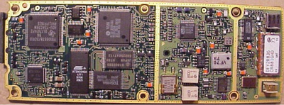
Today many designers are faced with trying to put more and more components in the same space of previously less dense assemblies. Knowing what the limits are means knowing what questions need to be asked to ensure the finished design will be buildable. There are many facets the designer needs to understand when trying to pack more in less space. They include component packaging, board size, land pattern design, spacing between components and, of course, the manufacturing equipment and process options, including testing. Too often one or more of these items are overlooked, resulting in escalated manufacturing costs or products that must be redesigned before they can be efficiently manufactured.
To head off potential DFM problems we need to consider all of the manufacturing processes and address them individually to understand how they factor into the making of a successful or poorly manufactured design. Remember, a successful design is one that is easy to manufacture and achieves the highest possible manufacturing yields.
Component Packaging
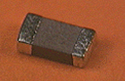
With advancement in technology, both active and passive components are available in smaller and smaller packages – some of which create a manufacturing nightmare. The selection of small packages, such as passives smaller than 0603, should only be used with approval from manufacturing (Figure 1). The 0603 can be wave soldered, but packages smaller than 0603 are typically suitable only for a solder paste print and reflow operation. In addition, smaller components such as the 0402 and 0201 will present placement challenges and can go beyond manufacturing tolerances at some assembly operations.
|
|
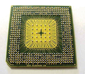
For active components choosing to use long centipede-like bodies or high lead count, BGAs can pose challenges to achieve an optimum reflow profile and should be discussed with manufacturing before routing (Figure 2). That’s not to say you cannot use these packages, but you need to consider on which side they should be attached, how the board will be handled through assembly and what processes they will need to go through. These are all critical to a successful outcome. Therefore, the package selection and placement should be reviewed with manufacturing before proceeding.
|
|
Be sure not to make assumptions because not all packages called out by the same case size have the same dimensions. Most of you are experienced designers who have already been bitten by that one. Note that nominal package dimensions work the best when making patterns.
Board Size
At first it may not seem like board size matters, but it does. What matters to manufacturability is how much a board expands or contracts over the breadth of the board’s surface relative to the CAD database. Typically we think of a FR-4 board as being able to expand/contract up to 1.5 mils per inch, but it is typically about 0.5 mils per inch. This value adds up very quickly because it is shifting where a land pattern is expected for stencil printing paste and for the placement of a component. Remember, your stencil was made from your CAD database so any pattern shift could be opposite that of a shift on the stencil. As an example, for a 10-inch board the pattern could be shifted by 5 mils along a side and 7 mils on the diagonal.
Other items that can also have significant effects on the pattern shift include panel design, board thickness and board shape. Panels that are routed and scored, thin boards and odd shaped boards can add significantly to the movement resulting in a need for fiducials to correct for the pattern shift and/or skew.
Land Pattern Design
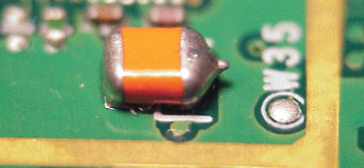
There are so many patterns for packages today that it is out of control for many of us. Which pattern do you use and when? We have the IPC patterns, libraries offered by independents and companies’ internal libraries. In addition, we have standard patterns, minimal fillet patterns (Figure 3) and filletless patterns (Figure 4). The standard pattern is most common, leaving enough plated surface exposed at the toe that a visible solder fillet can be seen up the terminal’s sidewall or lead. The minimal fillet has a barely visible solder joint and the filletless type has none at all.
|
|
|
|
The use of minimal fillet or filletless patterns has been popular for ten years in compact portable items such as cell phones. They require manufacturing to use an AQL plan in conjunction with X-ray to audit and control the process.
There are limits to manufacturing tolerances, meaning very small packages are to be avoided because they cannot be placed sufficiently onto a pattern. A well-designed pattern will control the part particularly during the solder paste reflow operation because metal wants to align to metal. Do not oversize the pattern because it will allow the component to move too much, causing it to shift off of the land.
Spacing Between Components
When it comes to putting distance between components, how close is too close? That is a good question and there is no set answer. The reason is that it depends upon the equipment, component package tolerances, board size, land pattern and the process being used to assemble the product. Ideally what you would want is a formula driven answer so that depending upon the variables you can plug in the numbers and come up with the correct answer. Several leading companies have found this works well, giving them some competitive advantage – therefore protecting this information. They built test structures and analyzed data to determine the correct values.
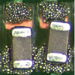
In studying some high volume assemblies I have found components placed a mere 7 mils apart, but this is an exception, not the minimum spacing rule for most product designs. Figure 5 shows components that are placed 6 mils apart. After reflow this placement resulted in a short.
|
|
Manufacturing Variables
A knowledgeable designer works closely with a team to accomplish successful high-density designs. The variables in manufacturing are many. They primarily consist of solder paste print, placement and reflow. This is not to say that other variables such as the ability to clean and test can be ignored.
Solder paste printing is one of the most critical steps in a process. If there are defects in the printing step they cannot be overcome later and will result in hand touch up, which is certainly to be avoided. Why? Rework increases the cost of assembly and lowers the quality of the finished product vs. having done it right the first time. Printing is critical because if the land pattern and the stencil aperture are not aligned the paste is printed off the pattern. The distance to adjacent components is reduced and possible defects, such as solder balling, bridging or even tombstoning can result (Figure 6).
|
|
Another key problem in printing is making stencils. When the distance of separation gets smaller the width of the stencil between lands goes down. The stencil’s web area becomes fragile and can easily be bent, particularly when non-contact printing is employed.
Component Placement Accuracy
Component placement accuracy depends upon the machine, maintenance, and whether vision alignment tools are required and used, or not available at all. I have seen excellent machines do poor placements simply because they were not properly maintained. In other cases components that really needed vision to compensate for pattern shift are not afforded the benefit of vision and therefore result in a higher-than-necessary touch up rate. When fiducials, shown in Figure 7, are required it is often advisable to check with manufacturing on where global fiducials may be used instead (Figure 8). Avoiding the use of too many component fiducials by using global fiducials improves repeatability. The distance between fiducials can be calculated with a pair of fiducials and in many cases can be used for numerous placements.
|
|
|
|
The Reflow Process
The reflow process is where all the lead gets soldered. If we have done our homework and applied it to our design it can help to widen the reflow process parameters, making it easier to assemble a product. In reflow we should be sensitive to how parts are oriented as they go through the wave or for some components through a convection reflow oven. Tombstoning and open solder connections were experienced a lot in the beginning of SMT in the early 1980s and it is once again showing up. Large components often heat unevenly. This results in one end of the component reflowing before the other end, causing the package to stand up on one end to resemble a tombstone.
Using high lead count BGA packages also affect the profile required to achieve reflow. Its impact needs to be considered in the placement review in conjunction with the manufacturing engineer.
Cleaning After Reflow
Of major concern is the ability to properly clean a dense assembly, especially when it has large components like BGAs on it. How the board will go through a clean system and whether it will be sufficiently cleaned is certainly affected by the type of system used, how closely spaced components are height-wise and whether shadowing will prevent adequate cleaning. This should be part of the placement review discussed earlier.
Testing
The goal is to have the product as thoroughly tested as possible. With so many nets and nodes on a large design the approach to test must be addressed in the beginning of layout. Test is a specialty skill area and having a knowledgeable test engineer review the design at placement is imperative.
Successful DFM is a team concept that needs to be employed in the design of high-density products. The skills of various departments are very important contributors and cannot be overlooked. The most critical time for review is after placements have been completed. At this time it is advisable to have the package selection and the physical locations of all the components carefully reviewed for all DFM considerations. When this review is complete and manufacturing has approved the placement, routing can begin. Following this process, you can avoid costly redesigns and other problems that are encountered on designs that are not reviewed. When problems show up too late in the design process it can result in cost overruns in assembly.
Building internally vs. using a subcontractor can make the review step easier. When the assembly is being built using a subcontractor be sure to tap into their skilled personnel to help you. Manufacturing wants you to succeed, because then they succeed too. PCD&M
James Blankenhorn is president of SMT Plus Inc. He can be reached at This email address is being protected from spambots. You need JavaScript enabled to view it..
