Short-Wire Test Fixtures Shrink Targets While Maintaining Integrity
More test points and shrinking real estate drive improvements in test tools.
Design engineers are adding new features to PCBs and increasing speed while reducing size and cost. The result is more test points and shrinking real estate, which means that the size of test points must be reduced. Meanwhile test engineers have the responsibility to ensure that boards work as designed throughout their useful lives. They want reliable and robust fixture technology to ensure a consistent test process. Smaller test probes are generally less reliable and require more maintenance in production. So test engineers naturally resist requests for smaller test targets.
These challenges are forcing a new look at in-circuit test fixturing technology. Traditional long-wire and wireless fixture technologies place the probe within a second larger tube called a receptacle that serves as a limiting factor on target size reductions. With new short-wire fixturing technology, on the other hand, the feature that holds and seals the probe is at the bottom of the probe, so the effective diameter becomes only that of the probe itself. This approach makes it possible for a probe formerly used on 0.050" centers to be used down to 1-mm (0.0395") pitch. Let’s explore the potential for addressing the challenge of shrinking test targets using this new technology.
Challenges for Conventional Fixturing Technologies
The inevitable progression of Moore’s Law is dramatically improving the performance and functionality of all types of electronic equipment, while at the same time putting increasing pressure on in-circuit testing fixtures to keep pace. The need to pack more test points into smaller boards is providing major challenges to conventional fixturing technology. The use of smaller test targets on finer pitches on most new designs is leading to lower first pass yields, higher test costs and sometimes generates bottlenecks that cause delays in beginning production.
The increasing use of ball grid arrays (BGAs) and other devices that restrict net access are creating additional challenges. Test engineers are pushing for design groups to migrate to boundary scan in order to test inaccessible points using long chains of data. Tests can include checking the connections between devices as well as locating any shorts between nets even if there is no physical access to these nets. The test program can eliminate physical access from some nets and free up board real estate for more circuitry and easier routing.
But several problems have frequently emerged when an effort has been made to take full advantage of the boundary scan technique. Long wires running from the tester to the in-circuit fixture can seriously deteriorate the signals that the board under test receives. Crosstalk between the wires can corrupt information chains, yielding false test results. Some test departments consider spurious noise to be a failure, boosting re-test and repair costs.
Evaluating Different Types of Fixtures
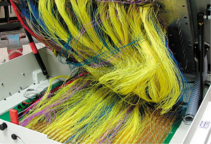
Such trends have forced many companies to take a new look at existing fixture technology. The two main types of fixtures used up to now have been long-wire and wireless styles. Long-wire fixtures have been the industry standard for over a generation and have the advantage of being familiar to nearly everyone. But long-wire fixtures require the use of receptacle-type probes that often make it difficult to reduce the size of test targets. Long-wire fixtures are also often associated with coupling problems and crosstalk because the long wires running from the in-circuit tester to the board interface unfortunately serve as very efficient transmitters and receivers (Figure 1).
|
|
Wireless fixtures were introduced about 15 years ago to address the limitations associated with long-wire fixtures. A multilayer PCB, called a translator board (T-Board), replaced the “nest” of signal wires. Double-ended probes connected the PCB to the T-Board. Wireless fixtures generally perform much more reliably than wired fixtures because PCB designers can intelligently control exactly how each trace is routed, making it possible to isolate troublesome signals. But wireless fixtures generally use the same probe technology as long-wire fixtures so they do not address shrinking test target concerns. Wireless fixtures also are more expensive due to the cost of designing and building the T-Board.
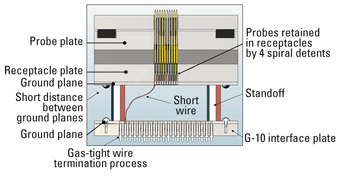
The new short-wire fixture uses a wiring module to route connections very close to the point where they are needed, shown in Figure 2. Removal of the hinge allows signal wires to follow a more direct path from the spring-loaded probes that contact and connect the PCB to the fixture interface. The resulting short wires are connected to probes retained in receptacles by four spiral detents. The probe has a recessed end that plugs into the receptacle, so the receptacle can now be the same diameter as the probe. Crimped connections are used on both ends of the wires that run between the module and problem. A gas-tight termination process is used in the wiring module, and a special tool has been designed to connect and crimp both ends of the wires. This tool is five times faster than the wire wrapping process used with long-wire fixtures.
|
|
Short-wire fixtures provide better signal fidelity than long-wire fixtures because the shorter wires have much less tendency to act as transmitters. Fixture suppliers have also introduced bi-level or dual stage fixturing to address situations where signal integrity is particularly critical. These products separate test points from in-circuit test problems. The test probes are mounted at two levels to eliminate the effects of having hundreds or thousands of antennas connected during functional test. During functional testing, only the probes necessary for the test are in contact with the PCB. Dual stage fixtures can virtually eliminate crosstalk between wires.
Improvements in Probe Size and Accuracy
Short-wire fixtures have also pioneered a new probe technology that eliminates the need to place the probe within a second larger tube or receptacle (Figure 3). The result is that probes formerly used on 0.050" centers can now be used down to a 1-mm pitch and probes used on 0.075" centers can now be reliably placed down to 0.050" centers without any concerns they will short together.
|
|
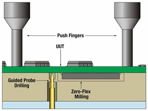
The new probe technology has excellent pointing accuracy, but the tips of the probes must be guided to provide optimal performance (Figure 4). An obvious opportunity to improve probe accuracy comes from reducing the size of the hole in the guide plate near the PCB. However, conventional probes make it necessary to provide considerable float in this hole because the plug that is press fit in the probe plate to provide a gas seal does not have any play. With short-wire fixtures, on the other hand, gas sealing does not involve the probe so the bottom of the probe is free to float. This makes it possible to size the guide hole significantly smaller to reduce radial endplay in the probes. Accuracy gains are achieved by controlling the probe plunger in close proximity to the test target. As a result, a 0.018" target can be reliably tested by the fixture. Headless probes must be used with this guide probe technology.
|
|
The new technology enables two types of probes and one type of receptacle to replace four types of probes and four types of receptacles in the traditional tube in a tube design. The new probe uses one probe to handle 0.100", 0.075" and 0.050" center spacing requirements and one probe to handle 1-mm applications. A single size receptacle is used for all probes. Standard technology would have required four probes with a unique size probe for 0.100", 0.075", 0.050" and 1-mm along with four unique receptacles. All probes fit into the same receptacle so fixture-wiring speeds can be improved, especially when high pin count fixtures are needed. The new design also offers a migration path for PCBs that will require testing on a 0.8-mm pitch. As with the larger sizes, the same receptacle is used with a spring probe to achieve this fine pitch capability.
The new probe technology helps alleviate the problem of robustness but fixtures must be more accurate to hit the smaller targets. New manufacturing techniques such as guided probes, diamond tooling and fine pitch drilling techniques have been developed to meet this challenge. Drilling is especially critical to ensure small targets can be accessed while avoiding the tendency for small test hole patterns to break out and allow test probes to short together. This limits qualified fixture manufacturers to those that have developed software tools and precision manufacturing methods. As a result, test engineers need to do more in-depth evaluations to ensure a successful project.
Avoiding Deformation
The PCB under test must remain flat for the probe to reliably contact small test targets. Localized deflections in the z-axis will cause the board to move in the x and y axes. Deflections on the PCB surface can also cause the test probe to deflect rather than penetrate the target, generating spurious results. There are two good methods of support: push fingers (hard stops) and zeroflex plates.
The zeroflex plate provides the most effective means of eliminating board deflection because the PCB is supported everywhere that it possibly can be. A zeroflex plate is created by milling a pattern into a push plate or support plate, or both, to provide clearance for components. Typically an extra 0.020" is removed from all surfaces to allow for any component float or shifting that may occur. CAD data and component information are vital to prevent damage to the PCB under test.
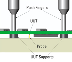
Push fingers with bottom side supports can also prevent board deflection as long as some additional rules are followed (Figure 5). To determine the number and position of supports that are needed, a board stress analysis that will identify areas of high deflection created by probe forces and high probe densities before the fixture is built should be performed. This information can be used to verify the necessary quantities and locations of fingers and supports to prevent excessive deflection.
|
|
Case Histories
The loss of PCB real estate created the need for small targets on closer centers, so a producer of networking equipment recently decided to try short-wire technology for testing the company’s newest products. This made it possible to shrink targets from 35 mils to 30 mils and reduce minimum center spacing to a 1-mm pitch. Typically fixtures have between 5,000 and 6,800 total test points and now also can have as many as 2,000 1-mm center probes. The new test rules were a great help to the design team. The fact that the more robust 50 mil probes were used for hitting the 1-mm targets helped alleviate some of the apprehension about switching to this new technology. The fixtures are working out very well.
A network equipment manufacturer-was able to substantially reduce bill of materials cost by moving to short-wire fixtures. The company previously had restricted design engineers to 0.050" centers in order to live within the limitations of the long-wire fixtures used in the past. Moving to short-wire fixtures made it possible to move to 1 mil pitch which in turn allowed the company to reduce manufacturing costs by using PCBs with fewer layers. The company obtains consistent performance from many duplicate fixtures.
Results such as these have made short-wire fixtures the preferred approach in a number of different applications. Compared to long-wire fixtures, short-wire fixtures enable smaller targets and greater signal integrity, albeit at a higher cost. Compared to wireless fixtures, short-wire fixtures also enable smaller targets at a lower cost. As a result, short-wire fixtures are normally the best choice in applications that use 0.050" or 1-mm fine-pitch connections. They are also ideal for boards with more than 2,000 test points because the wiring is so much faster. Short-wire fixturing technology can help electronic assemblers meet the challenges of shrinking targets and increasing point counts. PCD&M
Gary St. Onge is director of Global Kit Operations at Everett Charles Technologies. He can be reached at This email address is being protected from spambots. You need JavaScript enabled to view it.. Alan Albee is marketing manager at Teradyne. He can be reached at This email address is being protected from spambots. You need JavaScript enabled to view it..


