HDI Technology Moves Into Mainstream Design
Knowing when it makes sense to incorporate HDI into your designs will improve PCB performance, increase product reliability and meet established cost targets.
As electronics continue to become denser, the drive to produce more hand-held applications is obvious. However, portability is just one of many drivers for miniaturization. Fine-pitch packages and increasing pin counts of packages are the most important interconnect drivers in telecommunications, industrial, medical and military electronics. The proliferation of discrete components that accompany larger busses and terminations creates the need for embedded passives. Mother Nature is also playing a big role in determining the need for miniaturization as well. As chip signal rise-times continue to decrease due to smaller gate geometries, the resulting signals are more susceptible to interconnect parasitics. Further, signal integrity (SI) improves with miniaturization. All of these size-related factors are drivers for high density interconnect (HDI) with microvias.
Semiconductor complexity and increases in total gates have required more pins for integrated circuits (ICs) as well as finer pin pitch. Over 2,800 pins on a 1.0 mm pitch BGA is not unusual, along with 392 pins on a 0.50 mm pitch device. Faster rise-times, as well as the need for SI, require an increasing number of power and ground pins. Consequently, this drives the need for additional layers in multilayers and the need for HDI with microvias. One thing that is evident is that microvias aren’t just for cell phones anymore.
HDI is the interconnect technology being developed to respond to a diverse set of performance requirements. Microvias are the principal feature of HDI, along with thinner dielectrics and finer lines and spaces. This article covers the major drivers for HDI, when they should be used and when they are not appropriate, including:
- Integration of high-I/O and fine-pitch devices
- Higher component density and component I/Os
- Reduction in layer count for thickness control and RoHS compliance
- Improved electrical performance and SI
- Improved thermal performance
- Effective integration of embedded passives
- Lower costs through less layers and smaller boards
Deciding When to Implement HDI Technology
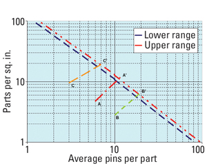
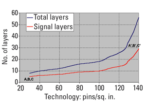
As discrete components continue to get smaller (with the increasing use of 0402s and 0201s) and IC packages shift towards more BGAs, the total number of connections on both sides of a board increase. When the average connections per square inch begin to exceed 100 pins (connections) per square inch (p/si), there is less room to wire these devices. The space occupied by the surface mount technology (SMT) land pattern, the through-hole via and the traces that connect them begin to exceed what you can put in a single square inch. This is the approach to the through-hole wiring barrier as seen in Figure 1a. Beyond 120 connections p/si, design rules have to be severely cut (resulting in lower yield) and additional layers added to complete the interconnect as shown in Figure 1b. The layer count begins to go up exponentially.
|
|
|
|
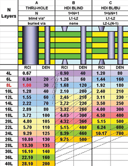
A summary of the HDI equivalents to through-hole multilayers is shown in Figure 2. RCIs are relative price comparisons (to a normalized eight-layer board) and DEN is the average connections per square inch that this structure can accommodate. The diagonal lines connect equal density structures. So, as an example, an 18-layer through-hole board with an average of 100 pins p/si could have been designed as a 10-layer HDI board (1+8+1) because it can handle 200 pins p/si. Or, it could have been designed as a six-layer HDI board with 2+2+2 (also 200 p/si).
|
|
Figures 1 and 2 have been used to highlight a common point: A density of 100 p/si is where designs cease to be viable utilizing traditional through-hole via stack-ups, and HDI becomes a legitimate alternative. HDI is inherently more expensive to manufacture than through-holes, so using it at densities lower than 80 p/si is not cost effective because it costs too much compared to drilled holes. Note, however, that benefits other than density were identified in the introduction. If these benefits have a significant priority in designs, they could justify the cost increase of HDI. This then, is the major tenant of the “When not to use HDI” question. The answer is, “When the density is low, or when 8~10 layer boards are sufficient to meet the circuit needs.”
High Frequency Performance
The characteristic impedance of single-ended microstrips, striplines, coplanar and differential signals is determined by the material’s dielectric constant and the board’s thickness stack-up and design rules. Signal attenuation is a function of the material’s dielectric loss, design rules and trace length. A variety of noise, such as ground bounce, switching noise, power supply spikes, etc., is a function of power supply coupling through the board’s stack-up, ground layers, design rules and material characteristics.
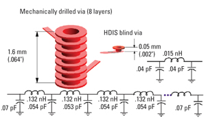
One of the major goals in improving the SI of a high-speed board is the reduction of inductance. The SMT mounting pads with the lowest inductance are without traces and use a microvia-in-pad (VIP). Figure 3 shows that a microvia has 1/10th the inductance and capacitance of a standard through-hole.
|
|
At gigabit data rates, all vias become very visible and unwanted components of the interconnect between driver and receiver. Microvias offer improved impedance matching, negligible reflections and minimized delay. They can also minimize electromagnetic interference (EMI). If a connection using the through-hole via in Figure 3 enters on layer 1 and exits on layer 2, the remaining via (layers 3-8) is an unconnected stub that radiates like an antenna. Microvias only traverse the layers requisite to make the connection, eliminating any stub effects.
Thermal Management
The thinner dielectrics that go with microvias are an aid to thermal dissipation. New films and liquid dielectrics also allow better thermal properties than may be found with conventional laminates.
HDI Reliability
Numerous reliability studies have been undertaken by the IPC’s TMRC for HDI structures, as well as many other organizations, such as Jet Propulsion Laboratories (JPL). These studies and organizations have all confirmed that properly manufactured microvias are many times more reliable than through-vias. Studies also indicate that the thinner dielectrics produce less stress on the via hole wall than classical through-holes do.
Increased Flexibility
Utilization of HDI technology increases the options available for a design. At a basic level, the options for layer connectivity are expanded greatly with multiple via structures. Traditional SMD, as well as advanced packaging technologies like direct chip attach, can be utilized. HDI is also an enabling, sister technology to other advanced technologies like rigid-flex and embedded passives.
Effective Applications of HDI Technology
The classification of products into HDI platforms is very much driven by the needs and recent progress in developing HDI products. Mobile communication companies and their PCB suppliers have been pioneers in this area and have set many standards. In parallel, product needs have pushed the limits of technology for high volume manufacturing and competitive pricing. The consumer industry in Japan had been far ahead in terms of volume manufacturing of HDI products. The computer and networking industry have not seen the high pressure of the past that goes with HDI technologies, but they will be forced in the future to set up the technology due to increasing component densities. The advantage of using HDI substrates in flip-chip packages is pretty obvious because of small pitch and increasing I/O counts.
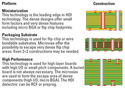
HDI technologies can be segmented in several technology platforms. The main drivers for HDI products today are mobile communication products, high-end computers and packaging substrates. The technical needs for these products are completely different, so that there is not one HDI technology but several platforms. Three platforms have been identified as:
- HDI for miniaturization
- HDI for very dense substrates and segmented functionality
- HDI for high layer count and local density
HDI for Miniaturization
The original aspect of HDI for miniaturization is the overall reduction of size and weight for the final product. This is achieved with the dense design itself, and with the compatibility with new dense components like µBGAs. An increase in functionality is possible in most cases while pricing is stable or even decreasing. The construction of this platform is mainly six or eight layers using internal connections (buried board) from layer 2 to (n-1). Other characteristics are a 10 mil via pad, 3-5 mil via holes, mainly 4-mil lines/spacing and a board thickness around 40 mil. The material is FR-4 or FR-4 with a higher Td (240°C). Figure 4 describes the basic construction configurations.
|
|
HDI for Very Dense Substrates
HDI boards for very dense substrates are mainly four or six layer constructions with buried via connections and two layers of microvias. The focus is to match the I/O density of the flip chips. This technology will soon merge with HDI for miniaturization.
HDI for High Layer Count
HDI boards for high layer count are conventional multi-layers with laser-drilled holes from layers 1 to 2 and 1 to 3 with sequential combinations possible. Microvias are drilled in the glass-reinforced dielectric or higher-performance, lower loss laminates. The focus is to escape out of component areas and to maintain the required impedance levels and electrical performance.
HDI has emerged from the halls of research as a viable, cost-effective technology for a variety of applications. But the majority of circuit needs today are simple enough that HDI is not a requirement. While increasing design density remains the obvious driver for HDI, the prevalence of high-frequency signals, increasing product reliability and thermal management requirements are also driving demand for HDI. PCD&M
Happy Holden is a senior technologist at Mentor Graphics. He can be reached at This email address is being protected from spambots. You need JavaScript enabled to view it..
