3D Thermal Modeling
Concurrent engineering tackles the thermal challenges of high-speed design.
The increasing density of high-speed PCB designs is making it more
difficult to simultaneously meet layout, signal integrity and thermal
requirements without missing market windows and incurring cost overruns
due to design re-spins. In response, Cisco Systems has defined a
temperature aware design flow that significantly improves co-design
between electrical and mechanical engineers. Designers begin by
transferring information from the PCB design software to thermal
analysis. A 3D computational fluid dynamics solver predicts airflow and
temperature for both sides of the board. Cooling management can thus be
considered from the earliest stages of the design process. Placement
updates made in thermal analysis can be passed back to PCB design,
providing bi-directional connectivity, which allows for concurrent
placement and thermal design.
With each successive
generation of Cisco products, increases in functionality and speed have
increased thermal design challenges. The power consumption of the
typical PCB has risen from 600 to 2,000 watts in just the past few
years, raising thermal design from a relatively minor issue to a major
design and reliability concern. In fact, at 600 watts the heat
dissipated from a PCB could not only affect mean time between failure
(MTBF) but even prevent the chips from functioning at all. The
traditional method of verifying thermal performance of new PCB designs
involved a considerable amount of manual transfer of information. The
hardware architect typically developed the block diagram floor plan
study in Visio. Various spreadsheets files were used to produce the
bill of materials and board stack-up. The bill of materials served as
the starting point for a spreadsheet used to calculate power
consumption. All of this information was calculated in different
software and stored in different files. When the information was
updated, no record was kept of previous versions nor was the reason for
the change recorded. The hardware architect provided this information
to the thermal engineer who entered the information into the thermal
analysis software and modeled the behavior of the PCB.
The
biggest problem with this approach was the amount of time required to
perform thermal modeling. It took about five days to generate
first-pass results and most of this time was spent manually entering
the data and going back to the hardware architect and other electronics
engineers to obtain missing information. Essentially, the thermal
engineer had to repeat much of the hardware architects' work by
transcribing it into a different format for analysis. The need to
re-enter information created the potential for error, either through
simple data entry mistakes or through misinterpreting the hardware
design. In other cases time constraints made it impossible to
incorporate all of the details in the design which sometimes led to
inaccuracies. Of course, while the initial thermal model was being
created, the board design had often changed enough to make the thermal
model obsolete by the time it was created. In any event, the PCB design
usually changed many times during the design process and usually it was
necessary to update the thermal model. These changes typically took
three to five days depending on their magnitude.
With
product cycles continually being reduced and thermal design becoming
more difficult, the inefficiencies of the traditional method were too
great to ignore. Cisco thermal engineers believed that the key to
improving this process was to automate the flow of information from
hardware design to thermal engineering. They learned of a tool with
features that seemed to offer the opportunity to improve this process.
This tool, called FloPCB, integrates with the PCB design software used
by Cisco. It promotes a new design flow in which information is
transferred seamlessly between the electronic and mechanical design
processes. The tool can be used by both electrical and mechanical
engineers to provide a single platform for information that is needed
during the thermal design process. This means data only needs to be
entered once and is available throughout the design process.
|
|
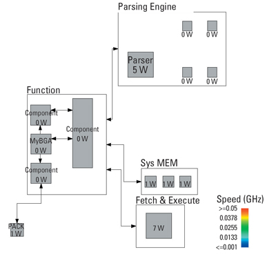
In the new design flow, the hardware architect
enters the block diagram into the new tool. The tool makes it possible
to specify connectivity between the various blocks that can be accessed
by the layout tool. Hardware design engineers can thus derive the first
physical layout directly from the block diagram. The bill of materials
and power dissipation values for each component are also entered into
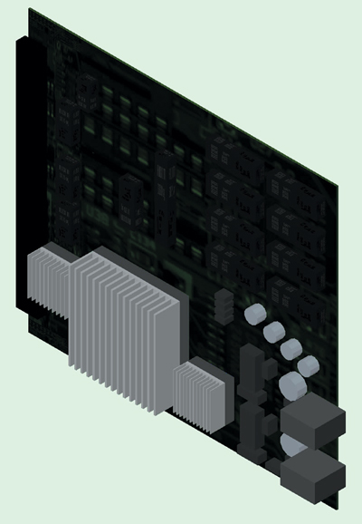
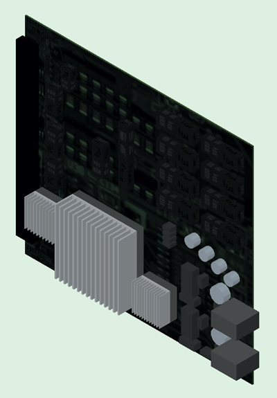
the tool at this point. The model is created in 3D from the very start,
eliminating the need for the thermal engineer to make the conversion
from to 3D (Figure 1 and Figure 2).
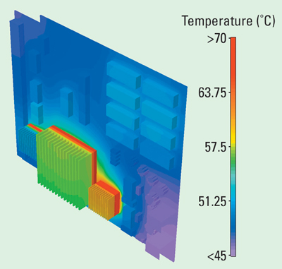
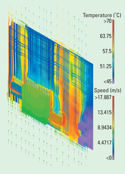
The mechanical engineer can perform a simplified thermal analysis from
this very early stage of the design process before the detailed layout
has been developed, using board level design to evaluate the new board
design in an existing system. A 3D computational fluid dynamics solver
predicts airflow and temperature for both sides of the board. Often the
design will identify hot spots, as seen in Figure 3 and Figure 4.
Identifying these problems at an early stage, before the first-pass
board layout is even created, makes it possible to correct cooling
problems at virtually no cost. Changes made during this phase to the
functional block diagram are immediately reflected in the physical
layout and thermal representation. This helps to keep members of the
electronic and thermal design teams in sync and enables them to
contribute to concept development in real time.
|
|
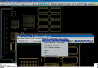
After the PCB layout has been completed, the
need exists to create a more detailed thermal model. Designers can
simply call up a menu item in design software and move the PCB detailed
design information into the thermal design tool (Figure 5).
The design information updates the thermal model, making it possible to
simulate cooling management with a much higher level of accuracy than
can be achieved with the block diagram information alone. The
information transferred includes the number of metallic layers, the
type of each layer such as signal or power or ground plane, the
coverage of copper on the board, and the location and power dissipation
of each component. The interface also allows the user to select the
appropriate layer used to derive the physical extents of the package.
Placement updates made during the thermal design process can be passed
back to design software, providing bi-directional connectivity for
concurrent placement and thermal design.
|
Moving to a System-Level Simulation
At
the early stages of the design process thermal engineers will typically
simulate the performance of the board under simplified conditions such
as constant airflow on each side of the board. These conditions work
well for basic tasks such as identifying hot spots. As the design
process moves forward, thermal engineers want to see how the board will
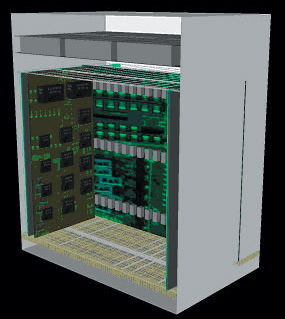
perform thermally under more realistic conditions. To accomplish this,
they usually import the thermal model of the board into a system level
model. At first, a model of the actual system will probably not be
available so engineers generally use a system level model that has been
created in the past for a product that is similar to the one being
designed. The system level model will generate thermal performance
parameters including junction-to-ambient thermal resistance,
junction-to-board thermal resistance and junction-to-case thermal
resistance as well as temperature profiles within the package under
various conditions. Later, after the enclosure and other mechanical
components have been designed, a system level model that represents the
actual board will be created. The results from the system level
analysis can also be exported to the board level simulation for use as
boundary conditions. This makes it possible to iterate on the board
design at a faster pace than would be possible if the thermal
performance of the entire system was computed on each iteration (Figure 6 and Figure 7).
|
|
The same model that is used for system level
thermal analysis can also be used to address electromagnetic
compatibility (EMC) issues far earlier than is normally possible. To
date, Cisco has not evaluated this application. The thermal model can
be used to perform an EMC simulation of the enclosure design to
evaluate its shielding effectiveness and identify which areas are
sensitive from an EMC standpoint. Because design often conflicts with
EMC design, fixes that are implemented to address thermal concerns
often exacerbate or create EMC problems. One example is that thermal
design requires large holes to enable adequate airflow while EMC design
requires small holes to reduce emissions. A hole will pass considerable
electromagnetic fields in and out of the enclosure if one or more of
its dimensions is equal to or larger than the wavelength of the field.
Being able to address thermal management and EMC issues within a single
environment makes it possible for mechanical engineers to get a head
start on the difficult design tradeoffs that are frequently required
between these two disciplines.
Case History
Cisco's
new Laguna Seca switches for optical networking helps service providers
deliver broadband services quickly and reliably. To ensure the best
balance of performance and reliability, Cisco needed to address tough
design and manufacturing challenges posed by the growing complexity and
thermal load of the design. The PCB needed to be routed carefully to
place heatsinks in the most strategic locations to maximize airflow
over board components for the most efficient cooling. Placement and
routing were also problematic because meeting performance requirements
for the new product required that the PCB be increased from six layers
in the previous generation to 20+ layers in the new design. The high
cost of manufacturing boards of this complexity level meant that late
cycle re-spins promised to be very costly - not only in terms of
engineering and prototyping resources, but also in time-to-market
delays. The design team used the concurrent electronic/thermal design
methods described here to streamline the PCB design process by
addressing and solving thermal issues from the beginning of the project
when changes are easy and inexpensive to make. Cisco estimated that it
saved $50,000 to $250,000 in engineering costs and brought the product
to market three to six weeks earlier than would have been possible
using traditional design methods.
It appears that the
five days that was required in the past to evaluate a prospective board
design from a thermal standpoint can be reduced to only two and a half
days or less. The tool is relatively new so it's not possible to state
with certainty that these savings can be achieved on a consistent
basis. The accuracy of the information used for thermal simulation has
also been improved, increasing the accuracy of the simulation results.
The savings are actually greater than this comparison reflects because
shortening the time required to perform a thermal evaluation allows
engineers to react faster and avoid putting additional time and money
into a design with thermal problems. The greatest benefit of all is the
additional revenues that can be generated by bringing the product to
market sooner. PCD&M
Herman Chu is technical leader at Cisco Systems. He can be reached at This email address is being protected from spambots. You need JavaScript enabled to view it.. Akhil Docca is an thermal applications engineer at Flomerics. He can be reached at This email address is being protected from spambots. You need JavaScript enabled to view it.. Sherman Ikemoto is business development manager at Flomerics Inc. He can be reached at This email address is being protected from spambots. You need JavaScript enabled to view it..
