The Impact of RoHS on Complex PCBs
Lead-free assembly puts a higher demand on complex PCBs.
The transition to lead-free wave soldering has brought with it many challenges. As with any new manufacturing technology entering a production environment, many of the associated challenges have been anticipated and prepared for in advance. Some of the challenges however, cannot be addressed until production volumes are high enough to flush out the problems and provide sufficient data and insight to work towards resolution. Often the engineering community continues to learn about the process as production ramps up.
Many people may not know that lead-free assembly processes aren't new. Lead-free wave soldering has been around for many years. Long before the RoHS legislation, electronics assemblies that experience high service temperatures used tin-silver solder because of its higher melting point. These assemblies were designed for harsh environments and were not very complex, so yields were acceptable. When RoHS requirements came to the mainstream of assembly, the first products to transition were also comparatively simple and included consumer electronics, utilizing single- or double-sided PCBs, with relatively trouble-free SMT devices on the solder side of the PCB. Transition of these types of assemblies was straightforward, as the process settings did not significantly differ from the tin-lead parameters. In many cases, even the original tin-lead compatible flux could be used successfully in the lead-free process.
We've learned over the last several years that the typical 0.062 inch (1.6mm) PCB will experience a somewhat tighter process window when going lead-free. The preheat requirements do not change very much, and most of the existing soldering systems are fully capable. The solder temperature can increase by up to 25öF, depending on the melt temperature used in the previous tin-lead process. The old tin-lead temperatures varied and I can recall years of wave soldering with the tin-lead pot set at 500öF. Hole fill can sometimes be more challenging with lead-free, especially with some of the OSP finishes. Dwell time on the wave may be a second or two higher. The drainage, or debridging properties, of lead-free solder is not quite as good as tin-lead, so finer pitch parts may present issues. All in all, most of the challenges seen on less complex assemblies have been easily addressed by developing the right parameter settings and using basic process control measures.
As thicker, higher-layer count PCBs and more complex assemblies (such as telecom infrastructure boards) make the transition, the difference between the tin-lead and lead-free processes grows. This is one of those areas where the engineering community can predict issues, but cannot study and address them until higher production volumes supply the necessary information. Now that some higher complexity assemblies are being produced in larger volumes, the challenges are becoming clear:
- The hole fill challenge seems to increase exponentially as board thickness increases.
- Higher layer counts and numerous ground connections exacerbate the hole fill issues.
- The higher thermal mass associated with the additional signal and ground layers create preheat challenges.
- If selective solder pallets are used, they shield areas of the PCB from preheat exposure, exacerbating the preheat problems.
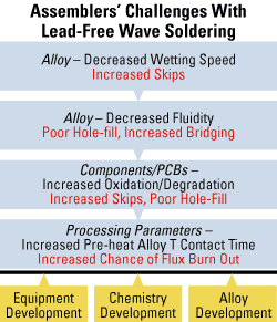
On simpler assemblies, a robust lead-free soldering process could be dialed-in by tweaking the existing tin-lead process. Basic DOE's or even trial-and-error methods would suffice at developing a high-yielding operation. This is not necessarily the case with higher complexity PCBs. To develop a robust process for more complicated boards, we need to gain a better understanding of the differences between individual factors in the processes. Figure 1 presents an overview of these challenges.
|
In Figure 1, the blue, downward pointing arrows itemize issues presented by individual aspects of the lead-free process. The yellow, upward facing arrows depict the improvements that are emerging in the market to address these new challenges and minimize their effects on yields and productivity.
Decreased Wetting Speed
Alloy wetting speeds vary among different alloys, fluxes and melt temperatures1. Although wetting balance test results do not predict wave solder performance, they do provide relative comparisons that demonstrate the effects of alloy composition, flux and temperature. The slower wetting speed translates to more skips on SMT devices and slower movement up the pins and barrels of PTH components. To overcome the slower wetting, longer contact times on the wave or higher melt temperatures are needed. The latter may not be feasible due to its possible detrimental effects on the components or PCB.
Decreased Fluidity
Lead-free alloys exhibit less fluidity than tin-lead ones. These solders take longer to wet up the pins and barrels, and are more prone to shadowing effects on components with improper orientations or spacing that is too narrow. Just like the effects of decreased wetting speed, the issues of decreased fluidity need to be addressed with longer wave contact times.
Decreased fluidity also translates to more solder bridges, as drainage upon peel-off from the wave is slower. Lead-free wave alloys are processed at temperatures much closer to their solidification point than tin-lead (only about 70öF higher in lead-free vs. 120öF in tin-lead), so the solder joints - and bridges - freeze faster. The faster solidification inhibits the use of debridging knives and makes the process even less forgiving, especially where poor design practices are involved.
With slower drainage, faster solidification and the absence of debridging tools, solder bridges must be addressed by concentrating on the peel-off area of the wave. Peel-off dynamics are affected by the speed of the conveyor, the height of the wave and the speed of the wave's pump. These parameters may require some fine-tuning to effectively debridge finer pitch connectors or quad flat packs.
Degradation of Solderable Surfaces
Oxide formation is a function of time and temperature exposure of the solderable surfaces. Here we have a classic example of the ongoing battle of good vs. evil: while the flux is trying to remove the oxides, more are forming. The higher preheat temperatures and longer times in the preheat tunnel increase the oxide formation on the leads, terminations and PCB, actively working against the flux that is trying to clean them. Oxides are barriers to wetting, causing lower hole fill and more skips. Again, longer contact times are needed to overcome these obstacles.
Processing Parameters
Increased preheat temperatures, preheat times, alloy temperatures and contact times all put new demands on fluxes. They must be capable of sustaining the harsher thermal excursions throughout the entire process. No-clean fluxes are formulated to activate and fully de-activate for reliability's sake in typical wave process windows. When a flux has been designed for the long, hot thermal excursions associated with lead-free high complexity assemblies, it may not become properly deactivated if it is used in lower technology applications that have shorter, cooler assembly conditions. The need for a flux to provide good soldering and remain reliable in this broader thermal range puts new demands on the flux formulators by widening their target operating window while simultaneously limiting their options for activators and other ingredients.
Compounding the Individual Effects
Slower wetting speeds, lower fluidity, more oxides and more aggressive thermal exposures all combine to make lead-free soldering more difficult. As the PCB gets thicker and more complex, the effects of these issues grow larger and interact even more.
Fortunately, solutions are continually being developed and introduced. Researchers around the world are studying new flux and alloy compositions to address the materials portions of the equation. Equipment suppliers are developing modifications to the mechanics of the process to help overcome some of the challenges introduced by the transition. And everyone is gaining process knowledge on an almost daily basis.
Many methods exist to address the known issues in wave soldering complex PCBs. Some of them tackle root causes, and others are more like "work arounds." In either case, they improve yields and limit rework. And certainly, as assemblers, equipment providers and materials suppliers quantify and understand these problems, more solutions will continue to emerge.
Increasing Contact Time
While increasing the contact time addresses wetting speed, oxidation and fluidity differentials to help improve hole fill and decrease skips, this practice has its downsides. Longer contact times heighten concerns of topside secondary reflow and copper dissolution. Additionally, slowing the conveyor enough to get adequate contact time may cause flux burnout in the preheat step of the process. In both cases the PCB is seeing a higher temperature for a longer time.
Nozzle designs to accommodate lead-free processes typically locate the turbulent and smooth waves closer together, have wider contact lengths and programmable wave pumps that increase the speed (and therefore the contact) once the boards have reached the wave and the danger of flooding it has passed. If lead-free soldering must be achieved with a tin-lead type nozzle configuration, the use of solder pallets may help. Pallets, due to their typical thickness and the location of stiffeners across the front, can run deeper immersion depths (and therefore longer contact lengths) without concerns of flooding the topside of the PCB.
Turning up the wave height may help improve hole fill, but it may also hamper debridging efforts. Recall that the peel-off is far more critical to debridging in lead-free soldering than it is in tin-lead. Increasing the pump speed or wave height changes the shape and flow dynamics of the peel-off. Hole fill and debridging may need to be considered in a trade-off. If the trade-off is necessary, keep in mind that even the most stringent IPC workmanship standard, Class 3, calls for minimum 75% hole fill. Topside solder fillets on through hole components could soon become considered a luxury of the bygone tin-lead era.
Preheat Considerations
Boards 0.093õ (2.4mm) and thicker must use topside preheat. On simpler boards, it is still possible to have robust lead-free wave processes without topside preheat. This is not the case with thicker PCBs. To assure fully activated flux, the solderable surfaces (including the topside annular rings) must reach a minimum of 212öF. If only bottom side preheaters are used, an enormous amount of heat energy must be directed through the flux on the bottom of the board and can de-activate it before the PCB reaches the wave. Topside preheaters help deliver heat from the opposite side of the PCB, providing the necessary heat energy without directly affecting the flux. When using topside preheaters, it is not uncommon to measure 285öF topside temperatures in order to achieve core temperatures greater than 212öF. The newer, convection-style topside preheaters are far more efficient at transferring heat than the traditional infra-red (IR) style.
Preheat temperature has always been a primary factor in wave soldering. Preheat time has not historically been a serious consideration, but when soldering complex boards in a lead-free process, it is very important. Slowing the conveyor enough to achieve the higher contact times needed to fill holes on thick boards can double the residence time in the preheat tunnel. The actual thermal profile should be considered. This means using thermocouples and dataloggers to measure temperatures, not shortcutting the measurement process with temperature sensitive stickers or handheld pyrometers. In the past, as long as topside or core temperature requirements were met, it didn't really matter what the profile looked like. But with preheat times (tunnel times) up to twice as long as tin-lead recipes, the impact on no-clean flux activity must be considered.
A common bottom side heater configuration is IR-convection-convection. One of the big advantages of the IR zone is its ability to allow the flux carrier to spread and dry slowly before the board reaches the convections zones, which can blow wet flux carriers off specific areas of the assembly. Historically, the IR panels have been run rather hot, delivering lots of heat early in the preheat cycle. The subsequent convection modules could run a little cooler (although the temperature settings are not readily correlated) and soak the heat into the PCBs. In the case of long tunnel times, the assembler may reconsider the profile strategy, and turn the IR temperatures down, allowing the convection modules to provide the majority of the heat. Although two zones of preheat may appear to provide even less heating capability than a three-zone tin-lead process on what may already be a thermally challenging board, this is not necessarily be the case.
Topside Reflow
Longer contact times at higher melt temperatures pose a greater risk of topside secondary reflow. Although the higher thermal masses of the thicker PCBs do absorb more heat, secondary reflow typically occurs on pads that are located near vias. When the hot solder fills the via, the heat travels through the trace to the pad and reflows the base of the existing solder joint. QFP and BGA lands located near vias are at the highest risk. Most design rules for distance from via to pad were based on tin-lead processing. Even though an assembly may have been properly designed for tin-lead processing, it may be more vulnerable in the lead-free process. When profiling complex PCBs, it is wise to locate a thermocouple on a pad that is near a via which has proper thermal relief and preferably does not tie into any heat-sinking power or ground planes.
Copper Dissolution
Rapid dissolution of copper into tin-rich alloys has implications for both the solder pot and the PCB. As copper levels rise in the solder pot, the liquidus temperature of the melt rises and fluidity decreases even further. As copper is washed off the PCB, traces and annular rings become thinner or nonexistent.
Pot contamination can be addressed through simple process control. The pot is initially charged with the alloy of choice (SAC305, -405 or -X0307, for example). It is recommended that initially solder samples be analyzed every 8,000 PCBs. When copper levels rise, the pot is replenished with copper-free alloy (SAC300, -400 or -X0300). In the simplest of control methods, the pot is sampled and replenished with copper-bearing or copper-free alloy based on its measured composition. In more sophisticated control schemes, the sampling rates are adjusted based on historical performance and the replenishment alloys can be predicted based on both historical performance and anticipated production loading.
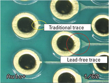
With respect to solder joint integrity, copper dissolution can be addressed though design practices. One of the most vulnerable locations on the PCB to be affected by copper dissolution is the trace that connects to the annular ring. It is typically about 6 mils wide, and a portion of it is exposed by the relief of the soldermask. To avoid dissolving this thin segment of copper, soldermask defined pads can be used. Alternatively, if metal defined pads are used, the traces should be made wider where the soldermask relief exposes them. Figure 2 shows a metal defined pad with wide traces that neck down underneath the soldermask.
|
Soldermask defined pads have presented reliability concerns in SMT devices, so naturally the question has arisen with respect to PTH devices. Although no reliability data is available on this design practice, it is becoming more widespread, and consultations with reliability experts indicate that there is no basis for serious concern.
It should be noted that although the wider traces offer some protection against copper erosion of the exposed portion of the trace, the "knee" - the area where the annular ring meets the barrel - is typically a bit thinner than the barrel or the ring, and can be very vulnerable to erosion. As of yet, no design or fabrication guidance exists to address copper erosion of the knees.
There is a common myth that avoiding the use of OSP surface finishes will limit the amount of copper dissolved into the solder pot. Discussions with metallurgists indicate that only electroless nickel-immersion gold finishes can limit copper dissolution rates due to the nickel barrier layer. Hot air solder level, immersion silver, immersion tin and OSP are all believed to behave similarly with respect to copper dissolution.
Alloys with higher silver contents like SAC305 and SAC405 are believed to dissolve copper faster than lower silver content alloys, and experimental data is available to support this statement. Continued experiments are currently underway to quantify the effects of surface finish, alloy type, melt temperature and dwell time on PCBs with both thin and thick traces exposed by soldermask relief. By the time this article goes to press, results of some of these experiments will have been published at the SMTA International conference.
Blow Holes and Voids
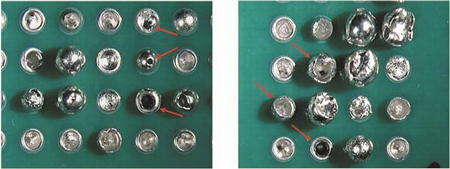
Figure 3 depicts a severe condition of blow holes2. In tin-lead processes, blow holes are usually formed by the outgassing of moisture in the PCB laminate through breaches or thin spots in the barrel plating, and they look like small pinholes or small volcano peaks. It is believed that they are formed by the same outgassing mechanism in lead-free processing, but the blow holes can often look more like balloons when the solder solidifies quickly during the outgassing process. The blow hole phenomena is far more prevalent in lead-free processing than in tin-lead. The melt temperatures are higher and the contact times are longer, exposing the PCBs to a greater thermal spike at wave contact, which creates more volatiltization and higher internal pressures.
|
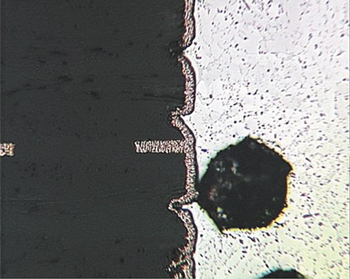
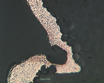
There are many unanswered questions about blow holing in lead-free soldering, and a root cause cannot be positively assigned at this time. There are several investigations that have led to the conclusion that the drilling process in PCB fabrication is a major, assignable factor. Figure 4 shows a cross section of the boards that produced the blow holes shown in the previous picture. The repetitive uneven pattern on the barrel wall may indicate that it was not drilled smoothly, and the plating process could not properly cover the uneven areas. A higher magnification of the uneven area is shown in Figure 5. The longer, hotter lead-free process is far less forgiving to plating imperfections than its faster, cooler tin-lead predecessor.
|
|
Barrel wall strength that is sufficient in tin-lead processing may not be sufficient in lead-free processing. This is evidenced by the fact that, in some cases, the same lot of PCBs form blow holes in the lead-free process, but perform to expectation in the tin-lead process. Multiple cases of this occurrence have been witnessed and reported. Failure analysis experts with over 20 years experience in the field report that nearly all cases of blow holes they have diagnosed are due to some form of poor PTH construction. Assemblers should consult with their fabricators regarding board specifications for the higher complexity assemblies that will experience the more demanding soldering processes.
There are no ideal solutions to address all the issues currently known, but understanding some of the mechanisms that affect these issues can help to limit their impact on yields and productivity. If trade-offs must be made, it is far better to make informed decisions rather than uninformed ones. PCD&M
Chrys Shea is manager of applications engineering at Cookson Electronics. She can be reached at This email address is being protected from spambots. You need JavaScript enabled to view it..
REFERNCES
1. Lifton, A., Bulwith, R., Picchione, L., Wetting Characteristics of Some Lead-Free Wave Solder Alloys, Circuits Assembly Magazine, July 2005.
2. Picchione, L. "Report of Analysis, Metallographic Examination of PTH Solder Connections to Determine the Cause of Voiding," CE Analytics, June, 2006.
3. Shea, C., Howell, K., "Process Control in Lead-Free Wave Soldering: Tighter Process Windows Need Tighter Process Controls," Proceedings of the SMTA International Conference, Chicago, IL, September, 2003.
