Next Paradigm Shift: Personal Mobile Phones
A case study in electronics miniaturization.
Over the past few years, there has been a dramatic increase in both the number and functionality of mobile electronics, especially mobile phones. However, mobile phones remain monolithic. Unlike PCs, they cannot be customized at the time of order, nor can you purchase add-on components. Based on the huge success of the personal computer paradigm, it would follow that mobile phones could also benefit from such as model. In this way one could take a generic mobile device and enable it to perform different functions by applying hardware "plug-ins." This would extend the mobile electronics envelope and offer flexibility and a customization component for the hardware manufacturers, suppliers and users.
A case study in miniaturization began with this goal in mind. The specifications of a mobile phone were set so all the functional components fit inside an SD card-sized module (32 mm x 24 mm x 3 mm) and the module itself could be plugged into a generic mobile electronics device.
Many challenges presented themselves in achieving such a degree of miniaturization. This case study presents the details of the entire process, starting from product specifications and concept designs to preliminary designs and performance analysis, and finally, to prototype production and functional testing. It also addressess many technical challenges such as antenna interconnect through the module edge connector, mechanical robustness and multi-chip packaging.
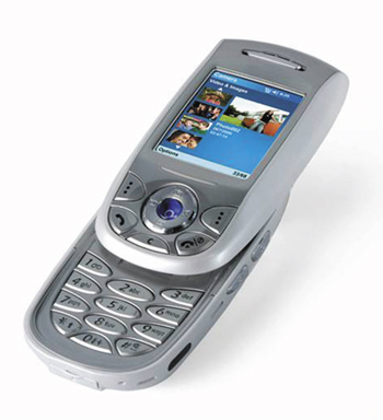
Figure 1 shows how mobile phones have evolved to become multi-function systems. This much functionality in such a small form factor was made possible through the miniaturization of electronics found inside the phone. But this system is largely integrated and not modular. One module found in this system is the memory card. This system is composed of many sub-systems such as telephony, MP3 player, video player and recorder, PDA, etc. Currently, the only module that can be replaced by a user is the memory (through the use of a memory card).
|
Almost all mobile systems - phones, PDAs and multimedia devices - fall under the category of fully integrated systems. This is analogous to the computing era before the advent of personal computers. The huge success of the PC industry is mainly due to the modularity of the system where a user can choose any component from multiple suppliers, whether they are motherboards, processors, memory, hard drives, etc. This has allowed thousands of companies to thrive with great benefits to the consumer in terms of flexibility, performance and price.
A similar approach can be envisioned for the mobile systems market where a consumer can customize their systems through a modular approach. The electronics of a mobile phone can be miniaturized and modularized to fit in a compact phone module (CPM). This card plugs into a phone that has only the case, keypad, display, microphone and battery. As these are common to many mobile systems, one could create pluggable cards for these applications and plug them into a bare system to make it function as a phone or PDA GPS receiver or MP3 player.
System Requirements
The requirements for the CPM were defined as follows:
- The card will measure 32 mm x 24 mm x 3 mm.
- It should be easily inserted and removed multiple times, such as the way memory cards are used. It will have a mechanical key to allow only one way of insertion.
- The card interface will be a combination of industry standard interfaces for functionally linking the digital and RF components in the card to outside peripherals such as antenna, display, keypad, battery, etc.
- The card will include a complete wireless modem, peripheral control and software functionality.
- Power management will maximize battery life.
- The card will be electrically shielded.
- The card has to be low cost, using standard FR-4-based substrate and one-sided assembly.
|
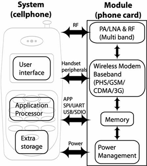
The block diagram for the system and module (CPM) is given in Figure 2. The module has all the components that define a complete wireless model, peripheral control and software functionality, plus antenna connections to enable host device with multi-bands and multi-mode wireless connection. The system provides the system case with user interfaces such as screen, keyboard, speakerphone, etc., a host processor for general tasks, extra storage and battery. Hence the system provides a generic computing platform with user interface and the module provides a specific function, such as wireless telephony in this case. The CPM connector should provide the following interfaces between the CPM and the host device:
-
n Handset peripherals. LCD, speaker, microphone and keypad. Color LCD with up to 18-bit bus and selectable LCD size and definition. Large enough memory to store drivers.
n Application processor. Compatible with major application processors such as Xscale, OMAP, etc., and UART connectivity.
n Antenna. Support 1.8-1.9 GHz through the CPM connector at 50-Ohm impedance with less than 0.5 db insertion loss and 5 W peak power.
n Power management. Self-contained power management in the CPM with bi-directional communication. Six pins to battery with ability to withstand 2A peak current at 3.0-4.2 V.
n Test and mode selection. JTAG interface for protocol software debug and upgrade.
CPM Design
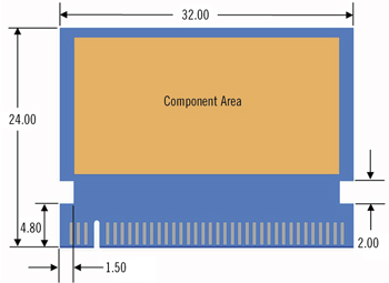
The overall CPM dimensions are 32 mm x 24 mm as shown in Figure 3. The connector portion is 4.8 mm. To allow for the EMI shield and for overall mechanical case, there is a 2 mm of keep-out area along the periphery. Hence, the component area is 28 mm x 17 mm (476 mm2).
|
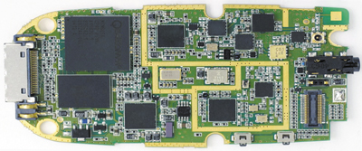
A typical mobile phone has the components shown in Figure 4. All the active devices and most of the passive components have to fit in the CPM (Table 1 [PDF format]). The area of the components listed in Table 1 is 400 mm2. As the component area on the CPM is 476 mm2, it is not possible to fit these components on the CPM and route the board. Hence, it was decided to make a 3D chip scale package (CSP) of the two biggest packages, the 240 IO baseband package and 48 IO Flash package.
|
CSP Design
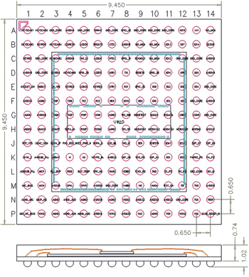
The 3D CSP design is as shown in Figure 5. The baseband die has 267 die pads and the flash die has 51 die pads. All the flash IO connect exclusively to the baseband die. Therefore, the number of solder balls for the 3D CSP can be reduced from 240 for just the baseband processor to 196 for the baseband and Flash combination. The package measured 9.45 mm x 9.45 mm with a 14 x 14 BGA at 0.65 mm x 0.65 mm pitch. By reducing the BGA count and decreasing the component count, the CPM board design was made significantly easier compared to the original cell phone board design.
|
The 3D CSP substrate was a two-metal with BT material as the dielectric. The design rules used were:
- Bond finger - 250 mm x 80 mm
- Bond finger to die edge - 80 mm
- Bond finger pitch - 125 mm
- Trace width/space - 35 mm/35 mm
- Via size - 80 mm
- Via land size - 200mm
- Via to package edge - 200 mm
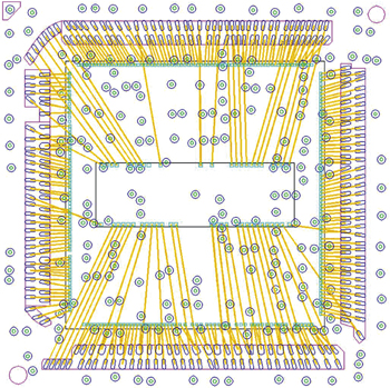
The wire-bond pattern was a challenge (Figure 6). Controlling the long wire-bonds from the Flash die to the substrate, especially the ones in the corners, required careful programming of the wire bonder. Also, to avoid excessive wire-sweep during overmolding process, the long wire-bonds were held in place by dispensing epoxy before overmolding of the package.
|
CPM Mechanical Design
The CPM should allow for easy user installment and removal. The connector should be able to withstand at least 250 insertions and removals. Most importantly, it should be cheap so that the total solution with the host device and the CPM is less costly than the original integrated host device. In other words, the savings in the board cost of the host device should offset the extra cost of CPM. As the original integrated design requires a 1-4-1 built-up board and the new modular design requires only a standard 4-layer board, the CPM does reduce the cost of the host device.
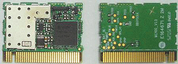
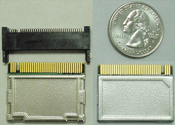
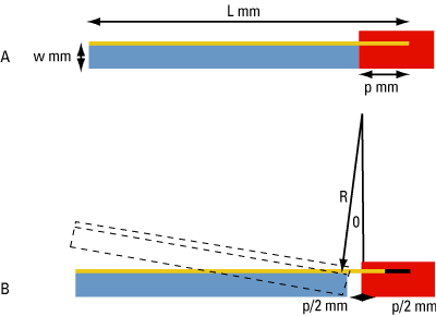
With this in mind, the CPM board was a standard board with an edge connector and a gap key to ensure insertion only one way. With the cooperation of the connector socket supplier, the connector length was minimized to shrink the CPM size. Also, the connector insertion force into the socket was reduced to allow for at least 250 lifetime insertions. This was done while keeping the electrical performance of the connector in mind, especially the RF connection. The finished CPM is shown without the mechanical cover in Figure 7 and with the cover in Figure 8. To ensure that the connector is robust under usage, simple mechanical analysis was done to properly design the mechanical guide mechanism for the CPM.
|
|
|
CPM with full insertion in an undeformed state and a fully deformed state with only half insertion are shown in Figure 9. The board next to the socket that has no mechanical cover is the likely failure point and the strain in that area is given as
|
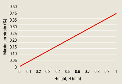
where t is the thickness of the board, H is the CPM edge deflection, p is the connector length and L is the CPM length. Figure 10 gives the strain as a function of the edge deflection. Assuming a maximum elastic strain of 0.2% for the board, the maximum safe edge deflection is H = 0.45 mm.
|
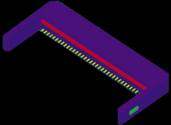
To ensure the card does not experience an edge deflection more than 0.45 mm, the socket that accepts the CPM was designed with arms that guide it in, controlling the amount of CPM edge deflection (Figure 11).
|
CPM Routing and Test Results
The CPM was a single sided assembly with the FR-4 board requiring blind vias for routing. Both the RF and digital signals were routed through an edge connector. An RF shield was placed over the 1.9 GHz RF section. All 167 components given in Table 1 were placed on one side of the board. In order to allow for high volume automated testing, key signals were brought to test points on the back side of the CPM as shown in Figure 7.
The 50 ohm RF signal was surrounded by two ground pins on the top side and three ground pins on the bottom side of the CPM connector. The RF interface was designed to support up to 2.5 GHz and 5-watt peak RF output power. The insertion loss of the edge connector was measured to be 0.60 dB at 1.9 GHz.
The CPM operated off of a single 3.6V supply and had an operating temperature range of -15°C to 65°C. The transmitter had an operating frequency of 1,880 to 1,930 MHz with 300 KHz channel spacing and a maximum output power of 10 dBm. The receiver sensitivity with a bit error rate (BER) of less than 0.01 was -102 dBm.
Conclusions
The CPM was designed, built and tested successfully. It measured 32 mm x 24 mm x 3 mm. The fully functional handset was demonstrated in February 2006 at the 3GSM World Congress 2006 Conference in Barcelona, Spain.
All the components needed for a complete wireless functionality including software, test and power management were included in the CPM card. The host device (cell phone) was a generic computing device with an application processor and user interface tools such as LCD screen, keyboard and microphone. The CPM met all the initial specifications including size, usability, performance and cost. A simple edge connector was used to minimize cost while maintaining adequate performance for the RF signals, which was 0.60 dB loss at 1.9 GHz. PCD&M
Ilyas Mohammed is manager, design, at Tessera Technologies. He can be reached at This email address is being protected from spambots. You need JavaScript enabled to view it..
