As smart integrated technology connected to the internet becomes mainstream across the consumables industry, complex design challenges are no longer limited to the elite innovating companies, but spread to the far reaches of manufacturers which juggle the trade-off between function vs. cost and competitive forces.
Wearable technology, like smart watches, are a prime example. As many players jump into the market to fight for the next great revenue growth area, they’ve got to up their game. Managing margins and pushing physical technology capabilities, to deliver a product with the correct price and functionality to reflect their brand positioning is a product design balancing act. Get it right and the pay-off in profitability is simple to see, the same applies for failure (no hiding behind rocks here).
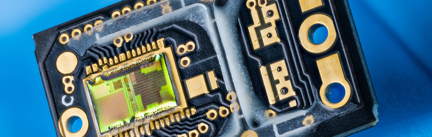
Case example: IoT enabled wearable technology. The unique characteristics of IoT and wearable products present some difficult design challenges. It’s the ages old story about delivering ever-increasing capabilities in smaller packages, but with the addition of more aerodynamic shapes. For example, the Pebble Smartwatch is only 43 by 34mm, or about one-fifth the area of a typical smartphone, and 10mm thick. An LED display, memory PCB, SoC controller, several sensors, Bluetooth chip, and a battery are all mounted on a double-sided PCB within the Pebble’s enclosure.1 In addition to their smaller size, IoT and wearable products often require contoured form factors and flexibility to accommodate the shape and movement of the human body, which further complicates the design process. The increasing functionality and shrinking size of IoT and wearable products also obscures signal integrity and thermal management challenges.
Advanced packaging adds fuel to the fire. The challenge is further complicated by increasing use of advanced packaging technologies to pack integrated circuits (ICs) more closely together in IoT and wearable products.
- Multichip modules (MCMs) are commonly used to achieve a small, thin form factor in smartwatches and smart glasses.
- System in Package (SiP) integration is being used to integrate digital logic, analog and RF subsystems into a single package.
- 3D-IC technology using through-silicon-vias (TSVs) is becoming common.
- Package-on-package (PoP) structures are being used to leverage packaged RAM while still reducing interconnect distance.
- PCB technology has also evolved over the years with high density interconnect, flexible and semi-rigid PCBs, and embedded passive and active components on inner layers, inside cavities and within the dielectric of the board stack-up.
The early bird gets the worm – mechanical and PCB integration. Early feasibility studies are required during product planning to realize best form, fit and function.
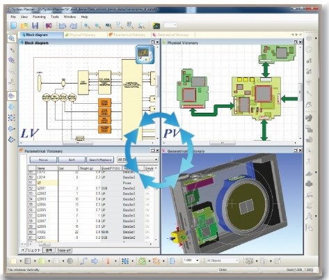
There is a greater need to focus attention on the critical early stages of the PCB and mechanical integration design process where requirements are translated to practical design decisions. Companies should be aiming for a virtual prototyping process where cost, number of PCBs, weight, size, enclosure fit and more can be evaluated collaboratively with the ability to make trade-offs before committing to detailed design. Why? Mostly because it significantly lowers delivery risk – as this is the stage where the product is configured and decisions are made, such as how many boards are in the system and what functions are on each board.
The new generation of design exploration tools provides a platform for concept and design creation through functional, 2D layout, 3D physical and BOM analysis views as well as preplanning board manufacturing aspects such as panel arrangement. Dynamic linking enables product planners to understand the impact of changes across every discipline involved in the design process. PCB designers have the ability to import the mechanical enclosure directly into the layout so they can ensure their layout meets the form factor requirements. By importing accurate 3D enclosure and component models, engineers can create board outlines, design to the actual 3D enclosure as a constraint, and conduct interference checks to optimize multi-board floor planning and design.
References
1. Howard Sian, "IoT and Wearable Devices Mean Rethinking Memory Design," Embedded.com, Oct. 19, 2014.
Humair Mandavia is executive director of Zuken’s SOZO Center in Silicon Valley.
Ed.: This post appeared first on Zuken Blog.