Enabled by superior materials, a host of passives have greater electrical benefits in even smaller packages.
Embedding a portion of the distributed capacitance within the substrate for general decoupling results in reductions of both board size and the number of on-board components. Additionally, improvements in electrical performance, such as EMI and noise reduction, lower impedance, and lower ripple, can be realized by embedding discrete components within a PWB. Despite these advantages, embedding is most often reserved for function- and size-critical designs due to the fact that the evolution of smaller form factors for standard ratings has permitted populating a printed circuit board with discrete parts to remain the standard assembly method for a large portion of consumer devices.
Passive components occupy the majority of board space on a PCB, even as the (dramatic) trend toward downsizing has continued via lower voltage digital applications coupled with increasingly volumetrically efficient materials. Embedded passive components can be formed by incorporating dielectric materials into a PCB or placing discrete devices inside cavities within the board and then burying them with additional PCB layers. The two most common capacitor technologies that lend themselves to ultra-thin embedded designs are multilayer ceramic chip capacitors (MLCCs) and tantalum chip capacitors. However, a relatively new technology, multilayer organic (MLO) laminate RF devices, which include capacitors, inductors, and diplexers, has also emerged as a prime solution for embedded designs.
A PCB with a typical thickness of 0.8mm can support a passive component with a height profile of ~0.6mm. Because PCBs have multiple layers, however, a more practical height target for passive components designed to be embedded into a single layer is ~0.15mm. Thus, the range of component profiles ideal for embedding in a single PCB layer to multiple layers spans 0.15 to 0.6mm.
Several enabling technologies specific to various types of capacitor technologies have resulted in high-capacitance, low-profile components especially designed to satisfy this span.
Evolution of Embedded MLCCs
In terms of footprint, MLCC size reduction has progressed from 0402 to 0201, and 01005 to even smaller, typically in parallel with automated component handling capabilities. Note: The Imperial system of size designations for chips, based on inches, is now being replaced by a metric system, at least for the smaller sizes. So, an 0201 Imperial size (0.02" x 0.01") can also be referenced as an 0603 metric (0.6 x 0.3mm), the 01005 as an 0402 metric (0.4 x 0.2mm), and the new 005003 as an 0201 metric (0.2 x 0.1mm). So, although the 0201 metric is still at the early stages of adoption, a large percentage of automated handling equipment already demonstrates placement capabilities of approximately 30,000/hr.
Similarly, dielectric materials with smaller grain size and higher dielectric constant have enabled thinner layers that maximize capacitance at lower voltage ratings, even though the amount of active area within a particular case size is a smaller fraction of the total device volume. Paradoxically then, the current trend is for the median footprint for topside components to be smaller than the typical sizes used for embedded applications, in which 0402 and 0201 (Imperial) still predominate.
Embedded components have additional requirements compared to their topside counterparts, though, including a reduced height profile, which requires the thickness of both the body and the metalized termination to be controlled, and reduced parasitic electrical elements, which permit the components to operate as an ideal component over a wider frequency range.
The traditional construction of MLCCs, which have terminations plated over all five sides on each end of the component, ultimately ends up having a “dog bone” configuration, meaning each end is significantly thicker than the component body itself. For example, for an 0402 (Imperial) part, the typical termination thickness may add 20µm max (with a standard deviation of 2µm) to the top and bottom, which represents over 20% of the thickness for a 0.15mm profile device.
For capacitors, a new termination method – fine copper termination – has yielded a high-precision flat, thin copper termination. FCTs are achieved by seeding the exposed electrode area (rather than the entire end of the component) with a layer of palladium, over-plating the same area with a precise copper termination, and then adding an external layer of tin, tin/lead, or gold. This process results in a typical termination thickness of 8µm, with a standard deviation of 0.5µm. Examples of ultra-thin MLCCs produced with fine copper terminations are pictured in FIGURE 1.
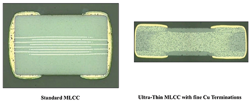
Figure 1. A comparison of standard (left) and ultra-thin FCT (right) capacitor terminations.
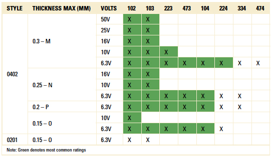
By enabling extreme control over termination thickness, the FCT process maximizes the ceramic body thickness, permitting ultra-thin capacitors to readily achieve the 150µm target and still retain high bulk capacitance values (up to 100µF at 6V) in an X5R dielectric. Other commonly available values of X5R dielectric capacitors suitable for embedding are listed in TABLE 1. This matrix shows available capacitance as a function of case size, component thickness, and operating voltage, and is expected to continue evolving to include a larger number of cells available from all manufacturers over time.
Table 1. X5R Embedded Capacitor Range
Reduced Decoupling Capacitor Parasitics
One of the main applications for MLCCs is decoupling ICs, which is trending to lower voltage digital systems in which large bulk capacitance is required, typically with X7R and X5R dielectrics. An ideal decoupling capacitor can instantly transfer all of its stored energy to a load; however, in the real world, a capacitor will experience parasitic electrical characteristics such as equivalent series resistance (ESR) and equivalent series inductance (ESL), both of which delay energy transfer.
The location and method in which decoupling capacitors are connected to the Vcc and ground planes, in addition to their internal inductance, have a significant effect on decoupling performance. As such, embedded capacitors have the potential to substantially improve decoupling through layout optimization and capacitor configuration.
Two first steps toward achieving optimum energy transfer are to optimize the capacitor’s placement and connections to the circuit and to minimize the capacitor’s internal inductance. These strategies address a common design consideration: loop inductance. The current in a circuit is considered to flow through an idealized conductor loop with a given height and width, defining a loop area. In the third dimension, this loop has a given span that is perpendicular to the direction of current flow. To minimize ESL, the loop area must be minimized, while the loop span is maximized. This strategy led to the development of the reverse geometry low-inductance chip capacitor (LICC), which, when compared to an equal case size MLCC, has an effective current loop with a smaller area and greater span that reduces inductance by approximately 3 to 4 times. These same developments are also being utilized in the ultra-thin components pictured in FIGURE 2.
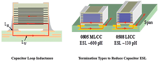
Figure 2. Inductance loop for signal path for different termination configurations.
A capacitor’s ESL results from the interaction of magnetic flux fields created, as current flows in and out of the device. As such, the ESL of a mounted MLCC directly relates to the area of an idealized current loop (LH x LW) formed within the board and capacitor. The current path (or loop) includes not only the multilayer capacitor’s internal electrodes and external termination, but also the power planes, vias, mounting pads, and traces (solder fillets and conductive paths) of the substrate and package (Figure 2). So, to minimize loop inductance between capacitor and IC, the decoupling capacitor should be embedded closer to IC and oriented on power (Vcc) and ground planes with minimal traces (Figure 2). This type of optimization is much more difficult to accomplish with discrete devices placed on the top and bottom of a PCB due to trace routing and physical distances to the IC. Following the assumption that decoupling capacitors can be optimally placed on Vcc and ground planes, a capacitor’s internal inductance plays a dominant role in decoupling efficiency.
Reducing Ultra-Thin Capacitor Inductance
In a simple analysis, there are two basic strategies to reduce the ESL of a capacitor: The first is to make the area of the current loop formed by the mounted device as small as possible, and the second is to employ multiple parallel loops to reduce the net inductance. Additionally, as previously stated, the same strategy that led to the development of the reverse geometry, low-inductance chip capacitor (LICC) is applicable to ultra-thin MLCCs. One example of such performance optimization is a standard ultra-thin MLCC that has been designed with “super lands” (large terminations) and an associated electrode to effectively reduce ESR.
With no technical impediments to production, other package styles of ultra-thin MLCCs will emerge as market needs appear. Low-inductance configurations available for ultra-thin MLCCs are shown in FIGURE 3.
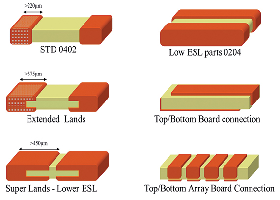
Figure 3. Ultra-thin MLCC terminations.
At the other end of the capacitance scale, low-capacitance, high-frequency capacitors are required for many RF applications, spanning Wi-Fi to antenna matching. Since high-frequency capability is associated with small capacitance values in the pF range, very small outline parts can be used to achieve this. The recent introduction of the world’s smallest copper (Cu) electrode, which is part of an 01005 Imperial (0201 metric) NP0 dielectric ceramic capacitor, achieves this, and the small form factor it enables makes the aptly named CU Series part ideal for topside and embedded applications alike. Cu electrodes also provide a low-resistance internal signal path that is optimized to reduce impedance and enable the highest Q 01005 MLCC available on today’s market for ultra-high-frequency (UHF) band applications spanning 300MHz – 3GHz. Another benefit of Cu electrodes is their ultralow ESR. With typical Q values of 290 at 1GHz for a 4pF capacitance, Cu electrode parts are ideal for reducing power consumption and improving battery efficiency in the high-frequency power amplifier circuits within multifunctional and multiband RF communication devices, including smartphones, tablets, camera sensor modules, and telecommunications equipment.
Together, these benefits have enabled a capacitor series that exhibits highly accurate and evenly distributed capacitances spanning 0.5pF to 22pF, which, combined with the part’s outstanding ESR, effectively mitigates impedance mismatching between circuits and subsequently preserves both power and battery life.
MLO Diplexers
Multilayer organic materials can be the carrier for an IC and create IC modules with total thicknesses less than 1mm. MLO can also provide an RF IC chip carrier substrate that is less than 0.25mm thick. The layer count for such a substrate would be six metal layers in order to support integrated inductor and capacitor elements capable of forming wide band diplexers, band pass filtering, baluns, and other circuit functions. In this configuration, thin MLO substrates can also perform decoupling functions through integration of high K dielectric cores.
MLO materials have been especially useful for developing small, low-profile diplexers suitable for embedding. Unlike relatively thick low-temperature co-fired ceramic (LTCC) diplexers, MLO diplexers are inherently thinner, making them more suitable for embedding in substrates. MLO materials offer some key performance advantages regardless of the specific component designed, though. For example, while designing MLO diplexers, a team of engineers gained valuable inductor and capacitor experience that resulted in an embedded 0603 high Q capacitor with capability up to 10pF and an embedded 0402 inductor with capability up to 82nH.
MLO components tend to offer very high Q and high current capability. Values of >350 for capacitors and >60 for inductors at 1GHz are not uncommon, and further MLO polymers that offer frequency capabilities to 100GHz have already been characterized. The MLO dielectric is piezoelectric-free and offers a low dielectric absorption (*3). Additionally, the thermal coefficient of expansion between the MLO classes of components studied is similar to FR4 PCB material (16 - 18ppm/˚C). MLO offers enhanced heat removal through the use of blind vias and through-hole vias, and material conductivity is >0.6w/k*m. MLO structures are also relatively easy to design, with extensive reliance on RF and electromagnetic (EM) modeling software, and are straightforward to produce through current PCB manufacturing techniques.
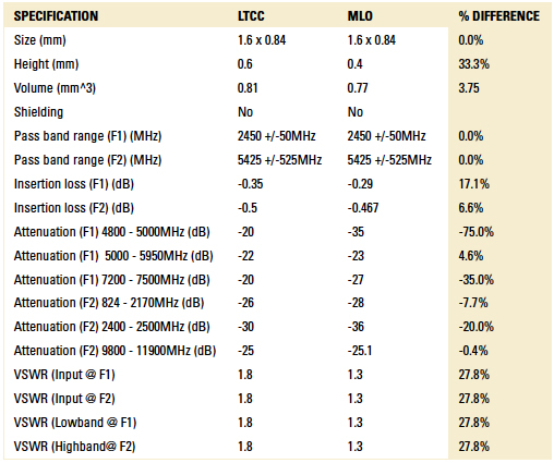
Due to the combination of these several beneficial characteristics, design engineers tried to create common band diplexers in an attempt to replace LTCC devices. Their results, summarized in TABLE 2, concluded MLO diplexers offer effective thinner alternatives to LTCC devices, and MLO diplexers have more attractive insertion loss characteristics and desired attenuation characteristics than LTCC diplexers. MLO materials are not without drawbacks, however, as their low dielectric constant limits large value components. As RF frequencies continue to increase, though, MLO devices have the capability to enable smaller parts with higher performance than devices built using traditional material systems.
Table 2. Specification Comparison: MLO Diplexers vs. LTCC Diplexers
Tantalum Chip Embedded Designs
Tantalum capacitors are essential in low distortion circuits and circuits that require a large bulk capacitance, and it should come as no surprise that embedded tantalum capacitors are needed to satisfy advanced designs. Thankfully, application conditions, material advances, and capacitor processing came together in a fashion that allowed development of an effective embedded tantalum capacitor.
From an application point of view, voltages have continued to drop from 5V to 3.3V, 1.5V and below. This evolution allows tantalum powder with extremely high capacitance per unit volume (CV/gm) to be used. For instance, values in excess of 200,000CV/gm are not unheard of. At the same time, however, customers have grown used to the continually improving reliability of tantalum capacitors, and have thus modified the traditional 50% derating factor to 20% in high-impedance circuits.
The primary feature responsible for limiting the height and package efficiency of tantalum capacitors is their conventional package, but the problem with scaling down conventional tantalum capacitors into embedded tantalum capacitors is twofold: efficiency and manufacturability. In a conventional molded J-lead package, the anode wire is welded to one side of the J-lead, and the cathode side is glued to a lead frame pocket with a conductive epoxy. The lead frame and mold area occupy a large percentage of the total package size, and, as overall package size drops, the volume of the package that is occupied by the anode begins to approach unacceptable limits. Additionally, the anode positioning within the package is critical in order to prevent areas where the anode is exposed to the outside via thin walls. So, as package sizes decrease to those attractive for embedded use, the anode positioning becomes even more cumbersome and demanding.
In response to these design challenges, a new manufacturing method similar to the one used in many parts of the semiconductor industry was developed to overcome tantalum capacitor manufacturing limitations and component value limitations. In this process, tantalum capacitor anodes are pressed onto a tantalum carrier, and, ultimately, the parts on the tantalum carrier are cut via diamond cutting wheels to singulate devices. So far, this process has resulted in the manufacture of the world’s smallest embedded tantalum capacitors: an 0201 equivalent case measuring 0.6mm±0.12mm in length and 0.3±0.06mm in both width and height. A comparison between the volume utilization of a traditional J-lead tantalum capacitor and a high-efficiency embedded tantalum capacitor is shown in FIGURE 4.
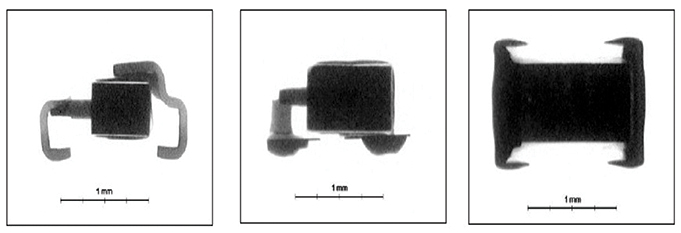
Figure 4. X-ray comparison of the volume utilization of a standard J-lead tantalum capacitor (left) and side and top views of a facedown style tantalum capacitor.
Electrically, these devices exhibit excellent frequency response characteristics due to the fact that parasitic inductance is eliminated from the tantalum package. For example, a 0.33µf capacitor can be built with a tolerance of +/-20% and a 100kHz of 35Ω, which is an expected value for such a small capacitor. AVX has demonstrated and manufactured 0201 tantalum capacitors with dimensions as small as 0.6 x 0.3 x 0.3mm and a CV capability of 1µF for 6.3V capacitors.
Manufacturing technology developed to achieve this part has also been used to produce a sub-0.6mm capacitor with a 1210 (3.5 x 2.8mm) footprint and CV capability as high as 100µF for 6.3V capacitors or 47µF for 12V parts. Such large capacitance values are currently ready to be embedded into thin PCBs, SIM cards, and express cards, among myriad other applications.
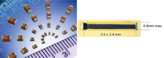
Figure 5. A miniature surface mount tantalum capacitor (left) and a cross-section of a 0.6mm max. height ultra-thin TAC embedded tantalum capacitor.
Summary and Conclusion
Advancements in ceramic, MLO and tantalum technology permit these materials to begin to address the challenging design demands of microminiaturization and embedding. The miniaturization of surface mount ceramic capacitors is expected to continue the trajectory presented; although, a new trend of more efficient ultra-thin ceramics for embedding should eventually offset the inefficiencies of extreme miniaturization. Additionally, a lower number of low-inductance ultra-thin embedded capacitors can replace a larger number of extremely miniaturized surface mount MLCCs. MLO structures can be formed into high-efficiency, high-power embedded capacitors, inductors, and diplexers, and, if given the right circumstances, could even be formed into a carrier populated with passives that the IC can be embedded within. Finally, miniature tantalum devices manufactured with new fabrication methods have enabled substantial size reductions, especially in the thickness dimension, which opens them up for embedding in substrates, especially since low IC operating voltages have lowered the derating factor designers apply to tantalum capacitors.
Chris Reynolds is technical marketing manager at AVX Corp. (avx.com); This email address is being protected from spambots. You need JavaScript enabled to view it..