Reducing signal degradation requires dielectrics with lower Dk and LT, more metal and conductors without rough surfaces.
At a trade show a few years ago, our Simberian booth was next to a booth with a very loud demonstration transferring 112Gbps over a distance of about one meter through cables. I don’t know how many terabytes of data they transferred during the show, but the demonstration equipment was noisy because of the industrial cooling equipment. I could feel the heat coming out of it. The devices were transferring data and not much else. How much energy is required to transmit data, and why is so much power dissipated into heat, I wondered.
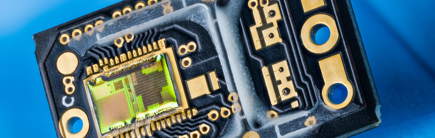
PCB interconnects degrade digital signals. Signals may be reflected, coupled to other interconnects, or to power distribution structures or free space, but most important, conductors and dielectrics always absorb the signal energy and dissipate or turn it into heat. This article is about signal degradation due to the inevitable absorption and dispersion caused by dielectrics and conductors. How much energy does it take to transmit one bit of information, and where does this energy eventually go?
With recycling efforts well below international targets, will manufacturers be forced to adapt again?
Environmental issues have been front and center in electronics for decades. Most engineers today remember when the Restriction of the Use of Hazardous Substances in Electronics (RoHS) first went into effect in July 2006.
Michael Kirschner is president of Design Chain Associates, where he helps manufacturers understand and ensure their products comply with health and environmental regulatory, customer and market requirements. He has broad expertise in areas including semiconductor quality and reliability, software design and development, hardware design, development, and manufacturing, as well as manufacturing processes and supplier/supply base management.
This background enables him to help manufacturers assess and improve supply chain risk, readiness and performance, and achieve compliance with REACH, RoHS, Circular Economy, EcoDesign, CEAP, WEEE and other related health, environmental and social regulations.
The annual trade show was slow by historical standards but attendees were pleased to be there.
The annual IPC Apex Expo trade show, traditionally the largest assembly show in the US, was more “expo” than “apex” when it resumed as a live event in San Diego in late January. Traffic was certainly lower than typical, and notably quiet at times. See what Covid hath wrought.
Several suppliers decided not to bring equipment. Some others cut back on the number of machines they brought. Many exhibitors reduced their employee headcount as well, leaving those East of the Mississippi at home and counting on their West Coast staff to carry the load.
Apex remains primarily an assembly equipment and materials trade show. The message from several SMT line vendors is Covid has led to diversification to North America from China, as companies can’t afford long lead times and face pressure to keep the IP of sensitive products in the West.
Effective strategies for calculating rogue wave noise levels.
For about 20 years, PDN design and analysis focused on the target impedance method. In recent years, additional considerations surfaced about rogue waves, but more as a general discussion. Here we present a new design/analysis method for estimating rogue wave amplitudes we can compare against the digital chip specs for design verification.
Electrical designs must be verified against possible worst-case conditions. For power distribution networks (PDN digital chip supply rail), this is typically done by comparing their impedance profiles against a target impedance requirement. From recent research and publications, we know the target impedance method for analyzing PDN design does not always predict the worst-case noise voltage because different frequency components of the chip supply current load steps can superposition on top of each other. This is sometimes called rogue waves (RW).
Written by Douglas Brooks, Ph.D., Johannes Adam, Ph.D., and Ulisses Castro
Category: Features
Signal traces internal to the board change temperature along their length, changing resistance.
In our recent book,1 an image shows how heat from a relatively hot trace flows downward through the board (FIGURE 1). What is important to recognize here is how little horizontal heat dispersion there is. The heat seems to flow straight down. What thermal images like this obscure is the relative horizontal and vertical scales. The horizontal width in this image is 50mm, while the vertical height is less than 2mm. Not enough room is underneath the trace for much horizontal dispersion. Consequently, the temperature of the bottom layer of the board directly under the trace is only a few degrees cooler than the temperature of the top layer, regardless of what is beneath the top layer.
RIT and industry have developed a novel curriculum for teaching PCB design. Is this the start of a college trend?
We are always interested in the approaches being taken to recruit and train the next generation of engineers. Readers may recall last summer we did a podcast with a group of recent graduates from the Rochester Institute of Technology’s Capstone program. There, the students conceive, design, source and build electronics hardware as part of a senior project. It’s truly a great way to immerse themselves in what a career in our industry could look like.
What we didn’t mention was RIT is launching another hands-on program. This one focuses on printed circuit board design. The first class started in January with 25 students. Chris Banton, director of marketing at EMA Design Automation, and Dr. James Lee, acting chair of the Electrical and Computer Engineering Technology department at RIT, explained what spurred the program and what it hopes to accomplish.