Making thermal simulation for electronics development faster, more efficient and intuitive.
Hotspots in electronic components are dangerous. To avoid discovering problems after thermal imaging of a prototype, thermal behavior is mathematically simulated before prototyping.
Conventional expert tools to calculate the thermal behavior of printed circuit boards use computational fluid dynamics simulations. Such tools generally require elaborate calculations using a 3-D model for the simulation.
A different approach involves a plug-in for a novel visualization and simulation tool. Under this approach, a 2-D printed circuit board layout is used as a starting point for the simulation, rather than requiring a 3-D model. Using ODB++ or IPC-2581 data, all relevant information for the circuit board design is loaded directly from the layout tool. For analysis, only the power dissipation of the components and the current values between the connections need to be entered, which generally takes less than five minutes. Following the definition of the procedure, for which the data are already stored in the layout tool, an analysis can be performed at the push of a button or automated using a script. A script engine makes performing a series of tests effortless. This makes thermal simulation no longer a separate process but rather a query based on the respective current PCB information.
Simulation at Zollner. EMS provider Zollner Elektronik uses the tool to optimize its development processes. Thermal simulation permits the early prevention of dangerous heat accumulation in assemblies.
Some practical examples: A filter board was simulated, which was intended to be tested later in the laboratory at 70°C. The 4-layer circuit board with 70µm copper coating carries two inductors with a power dissipation of 1.45W each. In FIGURE 1, yellow circles mark the inductors, and orange arrows mark the main current of 16A across the board. The simulation of the board showed a substantial temperature increase caused by the inductors. On the top layer, a hotspot of 94.4°C resulted at ambient temperature 70°C, and on the bottom layer the simulated temperature even reached 95.6°C (FIGURE 2).
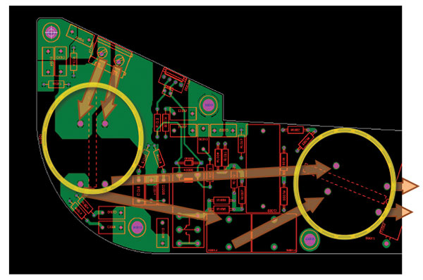
Figure 1. Schematic current flow on a PCB.
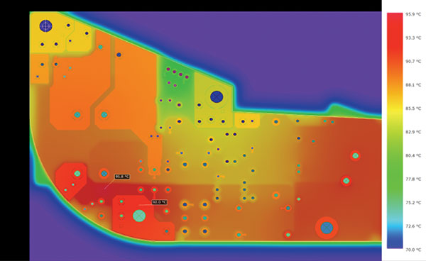
Figure 2. Thermo-simulation before adjustment.
The developers at Zollner adjusted the routing once more by adding copper areas to both innerlayers (FIGURE 3). The results of the new simulation confirm its success: The temperature remained below 85°C everywhere around the inductor L1001 on the left side (FIGURE 4), bottom layer following the adjustments). On the top layer, the resulting temperature was 10°C lower than in the first PCB version, which in turn has a positive impact on the temperature rise of the surrounding components. Using the simulation, it was possible to initiate and prove an effective improvement for the thermal behavior of the boards long before production of any prototype.
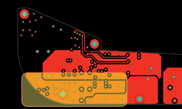
Figure 3. MID1-layer with additional copper surfaces.
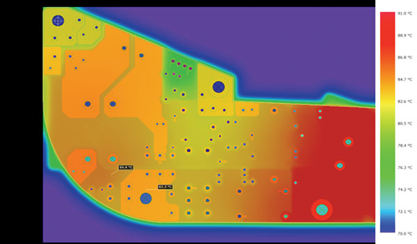
Figure 4. Thermo-simulation after adjustment.
“Without simulation, we would have to rely on trial and error using prototypes to achieve the optimal dimensions of the copper areas. This simple example already proves the value of thermal simulation, which we can now perform at the push of a button,” said Siegfried Reil, CAD application engineer DRL at Zollner.
Cross-functional and system-wide database. Zollner used the PCB-Investigator Physics plug-in, an extension of the CAD/CAM software EasyLogix PCB-Investigator. The software reads layout data in various formats (DXF, GenCad 1.4, Gerber 274x, etc.) and stores it independently of the otherwise used systems in ODB++ format. This creates a common database, documented in each amendment, for all users involved in the development, quality assurance and production processes. Any relevant known lifecycle data of the electronics development project are collected here.
Based on this, the plug-in simulates the thermal behavior. The engine within the interface is TRM (Thermal Risk Management) software from ADAM Research. Thus, the plug-in is able to incorporate multilayer boards, SMD heat sources, embedded components, pins, inlays, busbars, through-hole, pocket and buried vias. Comparing simulation and infrared thermal images of finished boards normally shows a very high match with a maximum deviation of ±10%, but typically better. Visualization of the simulation results even surpasses the thermal image in its informative value, because it also shows innerlayer hotspots, which thermal imaging would not recognize reliably. Based on the information provided by the CAD/CAM software, the plug-in illustrates temperature increases that are caused by currents and power dissipation of the components.
Günther Schindler is managing director at Schindler & Schill GmbH (easylogix.de); This email address is being protected from spambots. You need JavaScript enabled to view it..