-

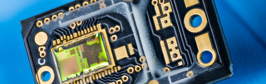
Thermal Vias are Ineffective. Here’s Why.
Adding thermal vias can take up valuable board space with little benefit.
READ MORE... -

Connecting the Industry, from Boards to Assemblies
HDP is embarking on new rounds of evaluations of laminates and lead-free solders.
READ MORE... -

Exploring the Impact of AI
A special panel discusses the growth of AI tools and its possible effects on the industry.
READ MORE... -
A Journey in Rigid-Flex Design
Overcoming the challenges of rigid-flex designs can be incredibly rewarding.
READ MORE... -
Creating the Ultra Library
Building and maintaining what's said to be the world's largest CAD database requires strong relationships.
READ MORE...
Homepage Slideshow
Thermal Vias are Ineffective. Here’s Why.
Adding thermal vias can take up valuable board space with little benefit.
Connecting the Industry, from Boards to Assemblies
HDP is embarking on new rounds of evaluations of laminates and lead-free solders.
Exploring the Impact of AI
A special panel discusses the growth of AI tools and its possible effects on the industry.
https://pcdandf.com/pcdesign/index.php/editorial/menu-features/17995-exploring-the-impact-of-ai
A Journey in Rigid-Flex Design
Overcoming the challenges of rigid-flex designs can be incredibly rewarding.
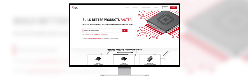
Creating the Ultra Library
Building and maintaining what's said to be the world's largest CAD database requires strong relationships.
https://pcdandf.com/pcdesign/index.php/editorial/menu-features/17914-creating-the-ultra-library