Improving SMT Assembly Yields
Solder bridging, PCB copper weight and surface finish: a cause and effect relationship.
Design tends to drive manufacturing, but both continue to push the limits of technology. A good design is one that meets, or exceeds, customer requirements while staying within the capabilities of manufacturing. Divergence from either will affect both.
The majority of defects in a surface mount technology assembly process are introduced at the solder paste printing process. These defects are not always immediately seen and are not solely due to the printer settings, solder paste, stencil or PCB. In some cases, the defects will not be identified until after pick-and-place or after SMT reflow, but, for many, the root cause can be traced to solder paste printing.
One such defect is solder bridging at reflow when printing PCBs with heavy/thick copper and/or a hot-air leveled (HASL) surface finish. The paste print can appear fine, visually, but the solder paste volume is larger than expected. In some cases, enough extra solder paste is printed to force solder bridging in reflow.
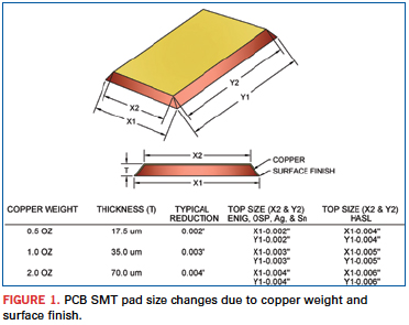
Etching of copper during PCB manufacturing will produce a trapezoidal cross-section (Figure 1) where the top of the SMT pad will be smaller than the bottom. Heavier copper weights are due to a thicker copper layer, and etching thicker copper will produce more of a size difference from top-to-bottom. The bottom (X1 in Figure 1) of the copper is where the measurements are taken during fabrication, and the bottom of the SMT pads will closely match the sizes in the digital PCB files. However, the top of the SMT pad is where paste is printed. Larger reductions at the top of the SMT pad, due to heavy copper etching, can make it more difficult to prevent paste from squeezing out between the PCB and stencil during print.
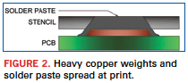
The majority of stencil design rules do not consider copper weight when determining stencil aperture reduction. The stencil aperture width is reduced by a standard amount, regardless of PCB configuration, and is typically tied to component pitch, component type or the SMT land pad size in the Gerber files. However, heavier/thicker copper weights can eliminate the gasket between PCB and stencil. In these cases, a more aggressive width reduction to stencil apertures is required to minimize the opportunity for solder paste squeezing out between the PCB and stencil (Figure 2). If the stencil aperture reductions do not consider the copper weight, the solder volume deposited at print can be quite higher than what is expected. In some cases, there is enough extra solder volume to cause bridging during reflow.
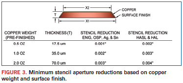
A similar scenario is created when using non-flat surface finishes like HASL and hot-air leveled (HAL). The non-flat surface makes it more difficult to create the gasket between the PCB and stencil and, again, solder paste can squeeze out between the two at print. A reduction to the stencil apertures, based on copper weight, is required, as well as an additional reduction when the surface finish is HASL or HAL. (See Figure 3 for recommended reductions based on copper weight and surface finish.)
Finally, incorporate PCB copper weight and PCB surface finish in stencil design. This cannot only solve potential problems at solder paste print, but also unforeseen problems down the assembly line.
Robert Dervaes is vice president of technology at FCT Assembly (fctassembly.com); This email address is being protected from spambots. You need JavaScript enabled to view it..
Have you registered for PCB West, the Silicon Valley's largest printed circuit board trade show? Sept. 24-26, at the Santa Clara Convention Center. www.pcbwest.com


