Best Practices for Improving the PCB Supply Chain
Printed circuit boards are a critical commodity. Here’s how to treat them as such.
Electronics quality and reliability are highly dependent on the capabilities of the manufacturer. Manufacturing issues are one of the top reasons companies fail to meet warranty expectations. These problems can result in severe financial pain and loss of market share. What a surprising number of engineers and managers fail to realize is that focusing on processes addresses only part of the issue. Supplier selection also plays a critical role in the success or failure of the final product.
Designing printed circuit boards today is more difficult than ever due to significantly increased density, higher lead-free process temperature requirements and associated changes required in manufacturing. Many changes have taken place throughout the entire supply chain regarding the use of hazardous materials and the requirements for recycling. The RoHS and REACH directives have caused many suppliers to the industry to change their materials and processes. Everyone designing or producing electronics has been affected.
PCBs should always be considered a critical commodity. Without stringent controls in place for PCB supplier selection, qualification and management, long-term product quality and reliability are neither achievable nor sustainable. Here, we discuss some best practices and recommendations for improving your PCB supply chain.
First, create a PCB commodity team with at least one representative each from design, manufacturing, purchasing and quality/reliability. The team needs to meet on a regular basis to discuss new products and technology requirements in the development pipeline. These meetings can take place through conference calls or via onsite visits. Pricing, delivery and quality performance issues with existing PCB suppliers should be reviewed. The team is also responsible for identifying new suppliers and creating supplier selection and monitoring criteria.
Second, establish initial PCB supplier selection criteria. The criteria should be unique to your business and products, but some general selection criteria include:
- Time in business.
- Revenue.
- Growth.
- Employee turnover.
- Training program.
- Certified to standards you require (IPC, MIL-Spec, ISO, etc.).
- Capable of producing the technology you need as part of their mainstream capabilities.
- Don’t build in process “niches” where suppliers claim capability, but little volume is built there.
- Have quality and problem-solving methodologies in place.
- Have a technology roadmap.
- Have a continuous improvement program in place.
Ideally, the suppliers demonstrate long-term stability from both quality and business perspectives. Multiple factory locations and risk mitigation programs can further protect against catastrophic political and weather-related events. After this initial screening, visit the PCB suppliers that seem to be appropriate matches. Site visits to the actual fabrication facility by personnel knowledgeable in PCB fabrication techniques are crucial. The site visit is the best opportunity to review process controls, quality monitoring and analytical techniques, storage and handling practices and conformance to generally acceptable manufacturing practices. It is also the best way to meet and establish relationships with the people responsible for manufacturing your product.
After choosing some potential PCB suppliers, the true qualification work begins. Qualifying a PCB supplier is always a two-step process. The first step is to qualify both a design and the PCB manufacturer through rigorous product and test-vehicle-based evaluations. The PCBs built for qualification should be evaluated to the standards you require by both the PCB supplier and your company (or an independent lab). The second qualification step is to initiate ongoing testing to monitor outgoing quality through a combination of test vehicle and lot qualification.
How do you verify a PCB supplier is capable of meeting your reliability requirements? There are currently six common methods for testing and qualifying PCBs:
- Modeling and simulation.
- Cross-sectioning combined with solder float/shock tests.
- Thermal shock testing (also
- thermal cycling).
- Printed Board Process Capability, Quality, and Relative
- Reliability (PCQR2).
- Interconnect stress testing (IST).
- Highly Accelerated Thermal
- Shock (HATS).
Very early in the design cycle, software simulation and modeling can be performed. As an example, DfR has implemented IPC-TR-579 into an automated design analysis software called Sherlock to permit rapid assessment of basic PCB robustness. IPC-TR-579 documents a “Round Robin Reliability Evaluation of Small Diameter (<20 mil) Plated Through Holes in PWBs.” This activity was initiated by IPC and published in 1988.
The objectives were to confirm sufficient reliability, benchmark different test procedures, evaluate influence of PTH design and plating, and develop a model. Some advantages of the IPC-TR-579 model are that it is analytical, validated through testing, and comments on the relative influence of design and material parameters. However, the validation data are over 18 years old. The model is unable to assess complex geometries, and it is difficult to assess the effect of multiple temperature cycles. The model also uses simplified assumptions (linear stress-strain above yield point). Finally, the model does not account for the effect of via fill and does not consider other failure modes such as knee cracking and wall-to-pad separation.
To successfully model a PCB design, the first step is to define the environment (Figure 1). Test, field or both environments can be modeled.
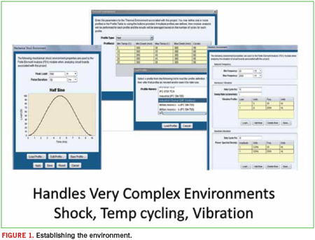
The second step is to upload the actual design information. Thermal maps can also be imported, if appropriate. The third step is to select the laminate and prepreg material. With this information, the stackup and copper percentage are automatically identified. Then, the PTH fatigue analysis can be performed.
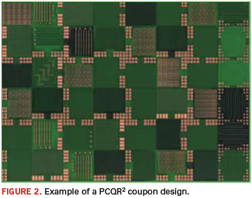
Another method is to qualify the design and manufacturer through the PCQR2 database and program. The program consists of a coupon design, a test standard, and a database of participating suppliers. The coupon has an 18" x 24" layout with 352 1" x 1" test modules (Figure 2). It can consist of two to 24 layers (rigid, rigid-flex) and requires builds of three panels and three non-consecutive lots with six times simulated assembly and HATS cycling.
An advantage of the PCQR2 program is that it is available in an industry standard (IPC-9151) format. It is easy to follow and provides real data for understanding PCB supplier capabilities (Table 1). It also provides a comparison to the rest of the industry through the use of an anonymous database. However, it is an IPC-approved monopoly and can be expensive, ranging from $2,000 to $5,000, not including panel costs, per supplier and facility evaluated.
Interconnect stress testing (IST) is the overwhelming favorite of high-reliability organizations for lot-based qualification testing. IST uses small (1" x 4") coupons that can fit along the edge of a product panel. Testing is automated, widely used and has the ability to drive barrel fatigue and post-separation failures. The large number of holes (up to 300) and continuous resistance monitoring make it far superior to cross-sectioning. And, in most cases, IST is a more cost-effective option. There are some potential issues to be aware of, however. The IST coupon design is critical. Preconditioning, test frequency, maximum temperature and failure requirements must all be specified. Test frequency can range from every lot to every month to every quarter. Maximum temperatures of 130˚, 150˚, and 175˚C are most commonly used. And, different markets and organizations specify different times to failure, with 300, 500, and 1000 cycles most common.
Next, if your product line ranges from simple to highly complex, consider tiering (low, middle, high) suppliers. Tiering permits strategic supplier selection to maximize cost savings and quality against your product design requirements. Match supplier qualifications to the complexity of the product. Some criteria for tiering suppliers include:
- Finest line width.
- Finest conductor spacing.
- Smallest drilled hole and via.
- Impedance control.
- Specialty laminates or construction needed (PTFE, flex, mixed technologies).
- Buried resistance or capacitance.
- Use of HDI, microvias, blind or buried vias.
- Minimize use of suppliers that outsource critical areas of construction. Again, do not exist in the margins of any supplier’s process capabilities.
Relationship management is another important element of success. Ideally, you are a partner with your PCB suppliers. This is especially critical if you have low volumes, low spend, or high technology and reliability requirements. Good partnering practices include:
- Routine conference calls between your PCB commodity team and each PCB supplier’s equivalent team.
- Quarterly business reviews (QBR) that review spend, quality, and performance metrics, and also include “state of the business updates.” Business updates can address any impending changes, such as factory expansion, move, or relocation, critical staffing changes, new equipment/capability installation, etc. The sharing is done from both sides. You also share any data that would help strengthen the business relationship: business growth, new product and quoting opportunities, etc. At least once per year, the QBRs should be site meetings that alternate between your site and the supplier factory. The factory supplier site visit can double as the annual onsite visit and audit that you should be performing.
- Ongoing supplier “lunch and learns” or technical presentations held at your facility or via webinar. Suppliers routinely provide education regarding their processes and capabilities. They can educate your technical community on PCB design for manufacturing, quality, reliability and cost factors. They can also inform you on pitfalls, defects, and newly available technology. This activity is usually performed free of charge, and suppliers may even provide free lunch to encourage attendance. It also gives you an opportunity to educate them on your needs.
- Supplier scorecards should exist and be used on a rolling quarterly and yearly basis. Typical scorecards include both objective and subjective metrics. Objective metrics include on-time delivery, cost, PPM defect rates, and quality excursions, which require root cause corrective actions. Subjective measures include communication issues (speed, accuracy, responsiveness to quotes) and cost-savings suggestions. And, there should be detailed discussion of any recalls, notifications or scrap events exceeding a certain threshold.
- Finally, make sure that any supplier has a robust continual quality improvement program in place. At a minimum, consider monitoring and reviewing the top three PCB factory defects, process control and improvement plans for those top defects, yield and scrap reporting for your products and feedback on general issues facing the PCB industry.
The foundation of a reliable product is a reliable PCB. Having a comprehensive strategy for selecting and qualifying PCB suppliers ensures the foundation is strong.
Cheryl Tulkoff is senior member of the technical staff and Craig Hillman, Ph.D., is CEO and managing partner of DFR Solutions (dfrsolutions.com); This email address is being protected from spambots. You need JavaScript enabled to view it.. DFR will be exhibiting in September at PCB West 2012 at the Santa Clara (CA) Convention Center.


