Putting these two under one roof provides OEMs greater assurances the end-product is successfully tested and avoids unforeseen problems.
PCB layout and test are inextricably intertwined. Some contract manufacturers maintain an in-house staff of layout designers, as well as assembly/test engineers. In such cases, the layout engineer delays creating all the necessary test points to avoid hindering routing. But once they finish critical routing and bus routing, an initial routing analysis and preliminary test points to achieve, say 50 or 60% coverage, they have the benefit of consulting with in-house test engineering to determine the right strategy to increase test coverage for the product.
OEMs that fail to take advantage of this basic and important practice when mapping out their system designs and manufacturing incur the greatest potential for extra costs, wasted time, and latent field failures. Consider the OEM that hands its printed circuit board design to a vendor located in one sector of the country. Then that OEM sends the electronic data (Gerber) to a fabricator at another geographic location. Afterward, the OEM purchases components and locates a third-party to perform assembly. Each stage – design, fab, and assembly – is distinctly separate from the others and, in effect, operates within its own confines with the OEM trying to successfully orchestrate the entire production cycle.
This process doesn’t make much business sense anymore, other than perhaps trying to save a few extra dollars. However, some OEMs still do this, especially those serving medical device and mil/aero markets, in which the slightest glitch can cause catastrophic consequences. Surprisingly, the consensus stance for doing it this way is simply, “We always have.”
What can go awry when opting for disparate operations? The OEM’s timeline, for starters. Consider the layout engineer at a selected PCB design house that performs only design and layout. Quite likely, they are involved with several design projects, each with specific completion dates. If that PCB layout engineer is behind schedule, causing a design to be late in delivering it to the fabricators, that triggers a domino effect with the fabricator experiencing unexpected delays, and delivery to the assembler (and market) gets compounded.
Murphy’s Law plays a role. Bad things do happen. The design and fabrication processes don’t quite jibe. The deliverables are not complete, or some critical information is missing, such as drill chart callouts or impedance control information. But the layout house argues that the problem rests with the fabricator. Finger-pointing continues until the problem is resolved, after much wasted time. Also, when using uncoordinated fabrication and assembly operations, the OEM fails to gain the benefits of highly coordinated resource expertise, which can be the difference between a product’s success and its failure.
Layout and Test Collaboration
Aside from these adverse issues, the crucial step of testing often gets short shrift when layout and assembly/test are vastly and geographically distant from one another. Ideally, a product gets the highest testing coverage possible – in the area of 85 to 95%. To accomplish those goals, having test and layout engineering under the same roof offers greater assurances they interact and jointly devise plans to successfully test the end-product. Experienced test engineers know all the nuances associated with in-house test systems. This is valuable knowledge that test engineers and technicians can pass to in-house layout engineering to be factored into designs.
It also helps when a seasoned layout engineer is familiar with flying probe and ICT test guidelines and limitations. For example, when a flying probe cannot reach a specific part of the board, that portion cannot be tested, thus reducing the test coverage. Then the layout engineer, keeping in mind those testing guidelines, can generate either more test points or use vias as test points to overcome that tester limitation (sidebar).
Testing is not jeopardized or shortchanged when PCB layout and test engineering maintain steady, orderly and productive collaboration. When a layout enters its final stages, the layout designer can transfer the CAD layout data to the testing department, where the testing access reporting mechanism can discern how much test coverage is actually available and on which kind of tester, keeping in mind the tester limitations. Here is where layout and test interaction pays handsome dividends. At this point, a series of mini conferences take place to discuss the steps the layout engineer needs to take to increase test coverage. Say, for example, test engineering determines a nearly completed design exhibits only 60% coverage. Since the PCB is still in the layout phase, the designer can use the new details and suggestions to add more test points or test vias, thus increasing testability access.
In this role, the PCB layout engineer must step out of their traditional design engineering routine and embrace a variety of test-related practices, procedures and disciplines, which need to be folded into the layout strategy at the placement, routing and finishing stages for a given board design. A classic example involves decoupling capacitors tied to an IC’s VCC or power pin. The smart PCB layout engineer ensures even distribution of those decoupling capacitors to help reduce noise. If the IC is not decoupled properly, locally generated noise ripples through the entire circuitry, creating jitter and ringing effects on the board. Those effects are later caught at the test stage, and the layout needs to be changed to reduce noise and jitter.
In another instance, the layout engineer must pay special attention when designing a high-speed bus that requires improved impedance and coupling control to satisfy the circuitry’s voltage and timing budgets. Special layout emphasis is critical for the bus design’s geometry and traces to develop proper test coupons. If not done properly, timing budgets will be off, and those mistakes will be caught at either debug or functional test stages, effectively too late for changes, short of re-spinning the board.
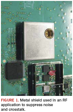
Also, in an RF application, signals generate parasitic coupling. The PCB layout engineer must implement ground shields or floods at the right locations in the layout to reduce parasitic coupling (Figure 1). Improving trace-to-trace impedance control is achieved by inserting ground shields between signal lines. This improves a uniform copper density across the entire board to ensure etch characteristics are equal to all signal lines. Again, if that’s not properly performed, test results send the layout back to the design for another go around.
Those are a few examples of what the savvy PCB layout engineer must know to successfully prepare a layout to achieve high-test coverage. Further, it’s important they fully understand the significance of such test procedures and characteristics as smoke test, gain and frequency response test, analog signature analysis (ASA), propagation velocity test, probing techniques, launch edge versus reflection edge, filtered TDR option, and others.
The smoke test is conducted to ascertain that data or signal aspects of the board are properly functioning. There are differences between a smoke test for digital and analog components. A smoke test provides some necessary assurances that system-under-test will not catastrophically fail. In other words, the circuit will not burn or systems will not crash. An example of the smoke test is the gain and frequency response testing. This involves measuring resistive points or loads between two different points to ensure they are balanced. The PCB layout engineer must understand this test because it helps prevent the circuit from burning, or at least avoids big mistakes from happening.
ASA monitors jitter, which occurs in digital ICs where the solid state jumps between two or three different points, thus causing instability. The experienced layout engineer will ensure a propagation delay between those two traces in order to make a stable state for doing ASA analysis, to control the jitter, and to ensure it’s within allowable parameters.
Propagation velocity testing involves propagation delay measurement and impedance measuring. Controlling impedance is relatively easy, and performing calculations and controlling a few factors to achieve impedance control is not difficult. But measuring propagation delay is considerably more difficult. Accuracy is extremely dependent on probing techniques dealing with connecting and terminating leads. Among the ones the PCB layout engineer needs to know about are handheld devices, SMA connectors, and controlled impedance micro probes, so they can factor in these test tools and considerations during layout.
As for launch edge versus reflection edge, the PCB layout engineer should have a firm understanding of this characteristic when doing high-speed designs. Last, filtered time domain reflects (TDR) option is used when excessive ringing occurs on a TDR response. Rise and fall edges must be aligned so they have zero time delay between rise and fall. Having this knowledge, the layout engineer is able to design the circuitry that is stable and has no jitters.
Sidebar:
Key ICT Guidelines
- Don’t tie IC control lines directly to power or ground. Add pull-up or pull-down resistors. This permits the ICT to control these lines when required during IC testing.
- Place test points away from BGA components to reduce BGA solder stress and board flex.
- Have a test point for all electrical nodes, including unused IC pins. This allows detection of internal and external shorts.
- To measure a low ohm resistor, two test points on each side of the component may be required to support 4-wire Kelvin resistance measuring.
- Oscillator should be gated with logic circuit, allowing ICT to disable the clock signal as needed during IC testing.
- Use boundary-scan-compliant devices when possible. This provides accessibility to the devices for boards with limited access test points. Also, chain multiple JTAG devices.
- If possible, place test points for each node on one side of the board (secondary side preferred). This reduces the fixture and maintenance cost. Top-side probing is less accurate than bottom-side probing.
Zulki Khan is founder and president of NexLogic Technologies (nexlogic.com); This email address is being protected from spambots. You need JavaScript enabled to view it..