For best results, know where to put solder mask, final finish and components.
Fine-pitch devices and automation levels are resulting in greater board density. There are mechanical and logistical limits to how far these trends can go, however, and the following best practices will help ensure that an SMT device is manufacturable.
For fine-pitch devices, designers must be careful to ensure that no natural bridges occur. A natural bridge is a clear, straight track between leads. This creates a trace over which solder can (and likely will) run when soldered (Figure 1). Although the result is not technically a defect, it appears as one to automated and human testers. This causes delays and additional manual (i.e., expensive) intervention to check. To avoid natural bridges, traces should be designed to route from the ends of pads, rather than using direct, straight connections.
Vias are holes drilled through layers of a PCB and plated to connect the layers of circuitry. Two design practices should be observed regarding vias and ball grid arrays:
Always mask vias under BGAs. Solder from the paste or balls on the BGA may come into contact with the via, creating a defect. Rework is problematic, as more heat is required to melt the solder. To avoid this situation, mask vias under BGAs with solder resist.
Avoid placing vias in pads. If a via is placed where a device is to be mounted, solder can run down the via, making rework difficult and reducing control over the solder joint volume.
Always ensure that copper pads define the solderable area, rather than using mask-defined pads. The mask application process is not as well controlled as the copper definition process, and defects are more likely to result.
Balance the thermal mass on leads of smaller devices, especially 0402s. Thermal imbalances can cause a defect known as tombstoning. In such cases, as one end of the device reaches temperature faster than the other end, surface tension on the molten lead causes the device to stand up on end.
Also, to achieve a flat PCB finish, organic surface protectants (OSP), electroless gold plating, or immersion tin finishes should be used on fine-pitch and BGA devices. This helps prevent defects such as open circuits on devices that contain many coplanar leads.
Solder resist dams of 0.003" are required, particularly on fine-pitch SMT devices. Omitting these dams increases the risk of short circuits through bridging between leads. The dams between these leads must be a minimum of 0.003" to be manufacturable by modern PCB fabrication processes.
Wave Soldering
The most economical method of soldering plated through-holes on SMT boards is with a solder wave machine (rather than manually). To help ensure that a board can be successfully passed through the wave, the following best practices should be observed.
Problems in manufacturing arise when a mixed board is heavy. Proper support and clear edges for stiffeners help avoid such issues. “Submarining” is a term used to describe the difficulties encountered when a double-sided board with inadequate support is put through wave solder. The board may sag, permitting solder to run across the top of the board and ruin it.
If a double-sided mixed-technology board is so dense that the above guidelines cannot be observed, a special fixture called a selective wave fixture into which the board is snapped can be used. This masks the bottom-side surface mount from the wave. To do this, there must be sufficient clearance (0.1") between the PTH pins and solder-side SMT so that the SMT can be masked by the fixture.
Keep in mind that fixtures add cost to the product, and it is best to avoid designs that require these. Several fixtures are required (at several hundreds of dollars each), and they have to be cleaned, loaded, unloaded and occasionally replaced.
Careful SMT pad design should be employed on the solder-side of a board. This includes thieving pads and toe pads, both necessary for successful wave soldering. In addition, components on the board should be oriented so that the solder joints are not shadowed as the board moves through the wave solder.
In all designs, snap-off materials should be designed on the edges of the board (Figure 2). These help support the board through the wave machine and can be removed after soldering. They also permit conveyors and clamps to function properly.
In some cases, titanium stiffeners can be used (provided there is sufficient clearance on the board) to help make the board more rigid. Both techniques require additional labor and therefore, add cost to the final product.
George Henning is vice president of manufacturing at OCM Manufacturing (ocmmanufacturing.com); This email address is being protected from spambots. You need JavaScript enabled to view it..
A common signal encountering the asymmetry that created it can cause noise.
Those familiar with designing high-speed single-ended interconnects don’t have a huge leap to design high-speed differential pairs. Both types of interconnects require controlled impedance, minimized discontinuities, low loss and short stubs.
But, one important new problem can arise in differential pairs that has no comparable effect in single-ended interconnects. This new problem can completely swamp the differential signal at the receiver and can make the difference between a robust product and one that works with boards from some vendors but not others. We call this new effect “mode conversion,” and it is related to the nature of signals on differential pairs.
It takes two transmission lines to transport a differential signal. We call the combination of the two transmission lines a differential pair. The differential driver that drives a signal on a differential pair has two output pins that create two different voltages on each of the two signal lines, with respect to their common return path.
These two independent voltage signals are usually denoted by either V1 and V2 or by Vp and Vn or by V+ and V-. They are the voltages between the signal line and the adjacent return path on each line.
For example, Figure 1 shows two voltage levels for an LVDS-type signal. Voltage coming off the two signal pins of the LVDS differential driver is called a differential signal, but this is a lie. Not all the signal is a differential signal: There also is a large common signal component.
By definition, the differential signal component is the voltage difference between V1 and V2. The common signal is the average value of the voltage. When we apply these two definitions to the LVDS signal, we see the differential component has a very simple form, and, in this case, a common signal is present, but constant.
If the two signals, V1 and V2, are perfectly symmetric – the same values, but exactly opposite – the average value will always be constant, and there will be no modulated common signal. If there is any asymmetry in the two voltages that make up the two signals, either in their voltage levels or their relative timing, some of the differential signal will be transformed into common signal. This effect is mode conversion: any asymmetry of any sort between the two signals that creates common signal and distorts the differential signal. This can arise from asymmetry in the driver or asymmetry between the two lines that make up the interconnect. No amount of distortion of the differential signal path will cause mode conversion, provided whatever is done to one line is done to the other. Of course, the differential signal could be grossly screwed up, but if so, there will be no mode conversion.
A difference in the cross-section between the two lines that make up the differential pair would change the impedance the driver sees looking into each of the two lines, and this would affect the voltages launched into the lines and generate common signal.
The most common source of asymmetry is a length difference between the two lines that make up a differential pair. It’s very easy to explore the effects of a length asymmetry on a differential signal using any circuit simulator that can perform a little algebra to show the calculated differential and common components of the signal (Figure 2).
As the length difference increases, the differential signal is degraded and a common signal is created. The most important problem with mode conversion is that the differential signal is degraded. Any length difference between the two lines in the pair will cause a time delay skew between them, resulting in some conversion of differential to common signal. And, this happens at the edges of the signal, which will directly impact the shape of the eye diagram.
A possible problem with the common signal arises if it were to get outside the enclosure of the product, on external, unshielded twisted pairs. It only takes about 3 µA of common current on external cables to fail an FCC Class B certification test. Less than 1 mV of common signal on an external unshielded cable will fail this test. That’s why every RJ45 connector to a cat 5 cable uses a common signal choke to dramatically attenuate common signals before they can be launched onto unshielded cable. However, if the common signal does not get out of the enclosure, it will rarely have an EMI impact. After all, every single-ended trace on a circuit board has a huge common signal without causing EMI issues.
Impact on Eyes from Mode Conversion
A more important secondary problem with mode conversion is that there will now be some common signal rattling along the differential pair. If it is not terminated, this common signal will reflect back and forth between the ends of the line. Since the receiver is sensitive to only the differential signal, rarely will the common signal cause a problem for the receiver.
However, if this common signal, in reflecting up and down the line, encounters the same asymmetry that created it, some of this common signal may convert back into differential signal, and this new differential signal, asynchronous with the initial differential signal, will be picked up by the receiver and look like random noise. Figure 3 shows the impact on a 5 Gbps PRBS eye for different line-to-line skews for the two cases of the common signal terminated and not terminated. When it is not terminated, the differential noise increases over the entire eye. When the common signal is terminated, it will not rattle around and will not contribute to asynchronous differential noise.
Terminating the common signal does nothing to prevent mode conversion and the distorting of the differential signal; it just keeps the reflecting common signal from distorting it further. Terminating the common signal will result in a cleaner eye, and the same amount of mode conversion will have less impact with a terminated common signal than without.
In all high-speed serial links, it is critical to terminate the differential signal, and this is always done with a resistor across the far end of the differential pair. The common signal, when reaching this far end resistor, will still see an open and reflect. To terminate both the differential signal and the common signal requires not one resistor but three (Figure 4).
To terminate the differential signal at the far end, R1 must be the odd mode impedance of the differential pair, typically close to 50Ω. To terminate the common signal at the end of the line, the parallel combination of the two R1 resistors in the series with R2 must be the impedance the common signal sees. After a little algebra, the value of R2 is found to be 0.5 x (Zeven – Zodd).
In loosely coupled pairs, the difference between the even and odd mode impedances is very small, so R2 is on the order of 1 to 5Ω. With this resistor network, the drivers will see an impedance of about 25Ω to the return path for the common signal. This will often mean a very high power dissipation, disastrous in many applications.
To prevent the DC power consumption but still provide an adequate termination for the common signal, a DC blocking capacitor is often placed between the center tap of the resistors and the return of the common signals. This network will terminate both the common signal and the differential signal. The implementation of this network and the resulting eye of a 1 Gbps PRBS signal with and without the common signal terminated are shown in Figure 5.
If there is so much asymmetry to distort the differential signal to worry about terminating the common signal, the way to fix this problem is to first eliminate the asymmetry at the source, then worry about terminating the common signal.
Too Much Skew?
Do not confuse line-to-line skew in a differential pair with jitter in the eye diagram. They are not the same. In fact, even when the skew is as long as 10% the unit interval, the impact on jitter in the eye is barely discernable.
It is common for high-speed signaling protocols to set a limit on the total acceptable line-to-line skew in a channel as less than 10% the unit interval. This includes all sources of skew, such as in the driver, the packages, the connectors, cables and the circuit board traces.
For a 1 Gbps signal, the unit interval is 1 nsec and a total skew spec might be 0.1 nsec. If this is all due to a length difference, using roughly 6 in/nsec as the speed of a signal, this suggests the total length difference that could be tolerated is 0.6 in. But, this is to be allocated to all circuit elements. If the board is allocated 10% of this total skew budget, the spec on the length matching for the board interconnects would be 0.060". As the bit rate increases, the total length skew allocated to the board would decrease.
For example, at 5 Gbps, this would be a total length skew limit of 0.012". When it is no longer free to match line lengths in a differential pair to this close a length, the skew budget would be renegotiated, or reevaluated. After all, a total skew of more than 10% the unit interval can be tolerated in many designs before the jitter becomes noticeable. At 5 Gbps, this is a length difference between the two lines in the pair of 0.120".
A second source of skew comes from the difference in speed between the signals in the two lines, as due to an asymmetrical dielectric distribution. This arises when one line in a pair sees more glass bundles than the other line and a higher Dk value, and travels slower than a signal in the other line.
This “glass weave”-induced skew is statistical in nature. It comes about due to the random chance that one line overlaps a glass bundle, while the other line in the pair sees a more resin-rich region. The magnitude of the effect depends on many uncontrollable factors, such as how well aligned the routing trace path is to the glass weave axis, the local variation in the Dk across the glass weave bundle, the pitch of the glass weave and the pitch between the two lines in the pair.
Controlling this source of mode conversion is about risk reduction. One approach is to keep your fingers crossed and hope for the best. Some designers have found this an adequate risk reduction strategy at 2.5 Gbps and hope it will also work at 5 Gbps.
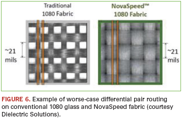
Another approach is to route the two lines in a pair on the same pitch as the glass weave. In typical 1080 or 2116 glass yarn, the weave pitch is about 0.021" along one axis. Routing the two lines in a differential pair on a 0.021" pitch will increase the chance the two lines see the same local Dk environment – either both resin-rich or both glass-rich.
Yet another approach is to use a glass yarn that is more uniform (Figure 6). In this case, the Dk does not vary nearly as much over the surface of the board, and the weave induced skew is dramatically reduced.
There are routing solutions as well: Don’t route along the glass wave axis; rotate the artwork relative to the edge of the board, or route with zigzags. All these solutions are to try to decrease the change of creating glass weave-induced skew.
As with so many signal integrity effects, problems get worse as data rates increase. While 1 Gbps systems have a high tolerance for skew-induced mode conversion, a 5 Gbps system is much more sensitive. Design approaches for 1 Gbps systems may not work at 5 Gbps, and it is important to reevaluate the design processes and constraints to verify robust performance in your next system design. This is why understanding the nature of the mode conversion problem, its root cause and the solutions available in your toolbox is more important each day. As we know, as speed goes up, luck goes down, but the more you know, the luckier you get. PCD&F
Eric Bogatin, Ph.D., is a consultant and founder of Be The Signal (bethesignal.com); This email address is being protected from spambots. You need JavaScript enabled to view it..
Segmenting the stencil layer improves solder coverage.
Quad-flat-no-lead (QFN) components (also known as MLF or micro lead-frame) used to cause a lot of problems a few years ago, if the number of blog posts covering the subject is evidence.1
Can I use my own blog as cited evidence to justify my own conclusion? It probably is bad form, but I’m doing it anyway. Interestingly, if you look up “citations” in Wikipedia, the entry (as of this writing) has a note indicating that the article on citations has insufficient online citations. Hmmm.
Anyway, it seems the industry is catching up with the proper manufacturing methodology for use of the technology. It’s important enough, though, that it bears repeating. The key to successful QFN and DFN manufacturing is in the solder paste stencil pattern. Consult the datasheet for the part, but if you can’t find the datasheet, or if it doesn’t cover the stencil layer, use the window pane technique, or “segmenting”, for the stencil layer when making the library part for the CAD software.
If the full thermal pad area is left fully open, the likely result will be too much solder in that area. The part will ride higher than it should and may very well float too high for all of the pads on the side to connect. (See the top drawing in Figure 1.)
Instead, shoot for 50% to 75% paste coverage by segmenting the stencil (Figure 2). That’ll ensure the center pad and the side signal lands will be at the same level. It will pay off in much better yields and reliability.
Duane Benson is marketing manager at Screaming Circuits (screamingcircuits.com); This email address is being protected from spambots. You need JavaScript enabled to view it.. His column appears bimonthly.
The age-old technology is seeing new life in medical and other applications.
Old technologies never die; they just get new names. Flex circuits have been around for many years in the IC packaging business and have been called almost as many names. In the early days, it was tape automated bonding (TAB). General Electric called it Mimi-Mod; Motorola called it Spider, and the first patent (despite an IP spat) was granted to a woman engineer, Frances Hugle, of Hugle Industries in 1969. TAB became famous with its use for driver ICs, connecting them to the ITO pattern on the glass LCD panel. The tape was Sn-plated, and issues with tin whiskers led Japanese companies such as Shindo Denshi to tackle the problem using an annealing process and nitrogen storage before bonding. Later the technology was called tape carrier package (TCP). Over time die were even mounted on the flex circuit without a bonding window, and the concept became chip-on-film (CoF).
In the 1980s, National Semiconductor licensed its TapePack technology to a several companies. This package also used TAB bonding. Kenzo Hatada at Matsushita developed a process called TB-TAB where a gold bump was placed on the TAB tape and die connected. Memory could be stacked this way. Other companies also worked on versions of stacked memory with flex circuits, including Thomson-CSF (now Thales). A 3-D package using flex is still in production today at 3D Plus, the spinoff from Thomson-CSP founded by Christian Val.
TCP was also used in Apple’s Newton. LSI’s ASIC was TAB-bonded in the package. The effort was the result of close cooperation among engineers with LSI, Sharp and Apple.
In the 1990s, flex became popular. A few ex-engineers (Tom DiStefano and Igor Khandros) from IBM got together and formed a company called IST. They came up with an idea to use flex circuit to make a really small chip-size package called a µBGA. They filed some patents, moved to California, and gave the company the name Tessera. Really, it was flex circuit. IC bond pads were connected to an array of bump connections on flex. Some DRAMs still ship in this type of package because this flex circuit structure provides excellent electrical performance. NEC developed a CSP using a flex circuit and called it a fine-pitch ball grid array (FPBGA). Nitto Denko used its ASMAT file with a z-axis conductive flex circuit material to form its Resin-Molded CSP. GE also applied its multichip module technology where flex was used for the redistribution layer to single-chip packages and called it a thin zero outline package.
Around 1995, Texas Instruments also came up with a CSP using flex circuit in order to make a low profile package called µSTAR BGA. This package is still in production. While these configurations were all single chip, flex circuit substrates were used for stacked die CSPs by Sharp, Fujitsu, NEC and many others because they provided an ultra-thin substrate that enabled a reduction in z-height. Tessera developed a folded, stacked package and Intel licensed it. This folder flex used a two-metal layer tape and was in production for many years until the business was sold to Marvell and the product reached end-of-life. Flex circuit substrate CSPs are being replaced by thin-core laminate substrates for new designs, but still accounted for approximately 1.5 billion packages in 2009.
Mainly driven by electrical performance, TAB tape was also used for large-size BGAs (TBGAs). Both TAB bonding and wire bonding have been used to interconnect pads on the die to flex circuit substrates. Semiconductor companies shipping TBGAs include Fujitsu, Freescale Semiconductor, NEC, Renesas and Toshiba. As rigid laminate materials have improved, TBGA volumes have declined.
While flex’s popularity seems waning in some IC packaging applications, it is increasingly popular in medical electronics. Hearing aids, catheters, imaging systems, some implantable devices, and other products depend on flex to meet space, performance and density requirements. The digital hearing aid is a good example. Flex is often a folded product, and depending on the number of folds, the overall length of the flex can be more than 1.5 cm with one or multiple arms and a width of 5 to 10 mm (Figure 1).
Flex is expected to play an important role in wearable electronics. One of a number of research programs underway in Europe, TIPS is targeted at medical and health monitoring both for implanted and non-implanted medical devices, sensors, and portable and wearable electronics systems. A folded thin flex module containing a hearing aid flip-chip set has been demonstrated.1
Flex already is playing a role in the embedded component business for a multitude of applications. The Imbera technology, known as Integrated Module Board (IMB), which embeds active and passive die in laminate structures, has been extended to flex circuits. A number of companies have developed processes incorporating resistors in flex circuit material, including Asahi Chemical Research Laboratory, DuPont, Ohmega Technologies, Ticer Technologies, and Endicott Interconnect. Buried capacitors in flex are offered by Oak-Mitsui Technologies, 3M Electronics, DuPont and Hitachi Chemical.
The flexibility of flex circuits will enable it to find applications in a variety of future products. New and exciting possibilities are expected of a technology that has been around a long time.
Reference 1. G. Kunkel, “Ultra-flexible and Ultra-thin Embedded Medical Devices on Large Area Panels, “ European Semantic Technology Conference, September 2010.
E. Jan Vardaman is president of TechSearch International (techsearchinc.com); This email address is being protected from spambots. You need JavaScript enabled to view it.. Her column appears bimonthly.
San Jose showed once again why it’s the epicenter for printed circuit design.
The outside temperature hit 103°F in the Silicon Valley, but inside the action at the PCB West trade show was even hotter.
Attendance at PCB West in late September was up markedly – 26% for the exhibition and 35% for the conference. Overall attendee registration jumped 20.4%, as the industry responded with vigor to the strong lineup of exhibitors, complemented by an outstanding technical program.
Signal integrity remained a major area of interest, although during the PCB Designers Roundtable – cosponsored by the good folks from the Silicon Valley Designers Council chapter – it was revealed that perhaps one-third of designers don’t actually perform SI analysis. (It’s left for someone else.) Proponents on hand, including the ubiquitous Rick Hartley, who taught several classes during the three-day technical conference, stressed that all designers should perform some level of SI. Also revealed: A large percentage of designers continue to manually route their boards, despite evidence showing autorouters could save time. Whether they do so because they are trying to protect their jobs is certainly understandable, but the notion that autorouting could free up resources that could then be used in other areas (such as SI analysis) bears consideration.
Many of the technical sessions that accompanied the trade show were packed, as designers and process engineers took advantage of the free sessions to glean valuable information on reducing layer counts, thermal management, post-assembly cleaning, and CAD-CAM. In one eye-opening presentation, Don Trenholm of Custom Analytical Services literally ran out of time showing slides of various counterfeited components.
On the show floor, several companies either showed new tools and services or discussed pending upgrades.
National Instruments (ni.com) is releasing an upgrade to its MultiSim and Ultiboard suite for design optimization, schematic capture and SPICE simulation. The new release will include upgrades to handle power components, simulation improvements, IPC land patterns, more user-defined functionality, and stronger encryption. “We are starting to bridge the point where we can do a design, the virtual testing and then see how they compare,” general manager Vince Accardi explains. (For NI, the show also marked a changing of the guard of sorts, as Accardi and longtime product manager engineer Bavesh Mistry have been promoted, and former R&D engineer Natasha Baker is taking over the latter’s role as PME.)
Mentor Graphics (mentor.com) touted its latest FloTherm thermal analysis tool, which helps designers identify thermal bottlenecks and shortcuts where new thermal paths would cool the design faster. The tool can perform a detailed simulation of the package itself, and users can overlay the component thermal model (which allows black box simulation) to simulate the package and complete PCB.
As long as there have been CAD tools, there have been translation problems. Not surprisingly, then, several companies showed various flavors of ECAD translators. SFM Technology’s PackageWright (packagewright.com) tool combines an online database of thousands of package models with footprint generation capability and an ECAD-MCAD library synchronization service. The tool supports flow from MCAD-ECAD and back.
AcAe (acae.com) drew a crowd with its DART ECAD conversion tool. Noting that the EDIF schematic and netlist translator format was launched more than 25 years ago, AcAe president Bill Basten said the biggest problem designers and manufacturers now face is that many translators simply don’t work. “The schematics don’t match; they can’t do constraints; they leave things out.” DART, he says, which runs on Linux and Windows, verifies netlists and copper, and permits use of libraries and symbols, provided they are similar.
PCB West has an emerging assembly bent to it, highlighted by several tracks on counterfeit component identification and mitigation, post-assembly cleaning and test strategies. Classes on thermal management and layer reduction were also popular.
By providing PCB engineers, designers, fabricators, assemblers and managers with the most targeted conference in the industry, PCB West proved the market for board-level shows isn’t dead after all. Full details regarding the conference and exhibition are available at pcbwest.com.
Following this year’s successful show, PCB West will return to the Santa Clara (CA) Convention Center Sept. 27-29, 2011.
Mike Buetow is editor-in-chief of CIRCUITS ASSEMBLY and PCD&F; This email address is being protected from spambots. You need JavaScript enabled to view it..
Measuring differential pair loss requires both lines to calculate the attenuation.
Whether a high-speed serial link channel works is just as dependent on the losses in the channel as its differential impedance. It’s not enough to just meet an impedance spec and verify it using a test coupon. In many applications, it is also important to meet a loss spec and verify the attenuation of traces in a test coupon.
Measuring the signal-ended impedance of a trace in a test coupon is easy. All fab shops understand how to do this with a TDR. It is tempting to think that if you use the same line in a single-ended line or in a differential pair, a line is a line, and all you have to do is measure it once to know the differential impedance. After all, the other line in the pair isn’t even touching its partner.
Unfortunately, while the proximity of the other trace in a differential pair will not change its single-ended impedance, the proximity will strongly affect the differential impedance of the pair.
Just measuring the single-ended impedance of one line in a differential pair, either as an isolated line or when in the differential pair, is no indication of the differential impedance. The measurement can be off by as much as 10% for tightly coupled microstrip or stripline pairs. You have to go the extra step to measure the differential impedance using a dual TDR.
Likewise, you cannot accurately measure the loss in a differential pair by just measuring the loss of one of the lines, or of an isolated version of that line. The coupling between the lines will affect the measured attenuation.
Figure 1 is a comparison of the differential insertion loss of a differential stripline pair, and of just one of the lines as a single-ended line stripline.
We usually define the losses in a uniform transmission line as the attenuation, measured in dB. Since the loss, in dB, increases linearly with the length of the line, it is often more common to use the metric of the attenuation per length, measured in dB/inch. For example, Intel recommends differential pairs used in PCIe III interconnects have a loss less than 0.78 dB/inch at 4 GHz.
In addition to geometry features, raw material and processing conditions will affect loss in a differential pair, making it necessary to measure test coupons to verify the attenuation per length of differential pairs on the board.
Unfortunately, measuring the attenuation of a single line that may be isolated or part of a differential pair will provide a different attenuation than the actual differential impedance of the pair. The coupling between the lines will affect the differential attenuation. Here’s why:
Loss arises from conductor loss and dielectric loss. In stripline, attenuation from the dielectric loss is independent of coupling. If there were no conductor loss, measuring the attenuation of an isolated single-ended line or one line in a differential pair would give the same attenuation as the attenuation of the differential pair. The attenuation from the conductor loss depends on the coupling in two ways. The attenuation is not due to just the series resistance alone, but the ratio of the series resistance to the differential impedance.
If the line width is kept fixed, and the two lines in a differential pair brought closer together, the differential impedance will decrease. Even if the series resistance were to remain constant, the attenuation would increase because the differential impedance decreased.
To complicate this further, the proximity of the two lines in the differential pair changes the current distribution in the conductors, changing the series resistance. Surprisingly, the series resistance goes down with tighter coupling as more of the return currents overlap and cancel. The current crowding in the signal traces does not start to increase the signal path series resistance until the spacing between the lines is much less than a line width.
The combination of these two effects means the attenuation will be higher in a differential pair than if measured as single-ended lines. This is all the more reason for all suppliers and users of high-speed differential channels to begin implementing a process to measure the attenuation of differential pairs for all high-performance boards.
Eric Bogatin, Ph.D., is a consultant and founder of Be The Signal (bethesignal.com); This email address is being protected from spambots. You need JavaScript enabled to view it.. His column runs periodically.