Suggestions for optimizing vias using circuit modeling.
Vias are a necessary evil in all multilayer circuit board designs. While even a poorly designed via can be transparent below 1 Gbps, for multi-gigabit links, vias can often represent the largest discontinuity and set the maximum bit rate that can be transmitted in a link.
The process to implement a transparent via in a differential path is to match its impedance to 100 Ω and eliminate any residual stub. Unfortunately, due to real-world constraints, it is not often possible to achieve 100 Ω, and removing stubs can be expensive. A practical approach is to do everything that is free, and then simulate to see if the design will work. If it will not, then it becomes worthwhile to pay for a closer match to 100 Ω or for shorter stubs.
The first step is do the best possible in the via design. Then comes the determination whether it is “good enough.” This requires having an equivalent circuit model of the via that can be incorporated in a system simulation. While one approach is to use a 3D EM field solver to generate a behavioral S-parameter model, this is sometimes expensive in time, cost and expertise required.
An alternative is a scalable, topology-based equivalent circuit model that accurately matches via behavior to a bandwidth well above the application bandwidth, typically above 10 GHz. Here, we look at a very simple way of modeling a differential via and translating its geometry into an equivalent circuit model.
A Differential Via
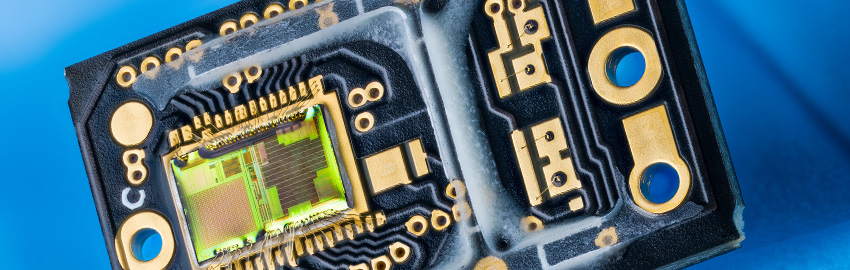
All high-speed serial links route signals as differential pairs. When the pair transitions from one layer to another, it does so through a differential via (Figure 1). Of course, it is always good practice to provide a “return” via adjacent to each differential via, but this is to provide a low impedance path for any common currents that might inadvertently be on the differential pair.

The differential signal will not see the return via; it will just see the two vias that make up the differential pair. The challenge is translating the via geometry into an equivalent circuit model that can then be integrated into a channel simulation.
One approach is to use a 3D full wave field solver. This approach will handle all arbitrary features of the vias, and include all ranges of layers, plane separations and clearance holes, offering the highest bandwidth and most accurate analysis. But, the resulting answer is not scalable. It is a behavioral model for the specific geometry selected, and must be re-simulated for all variations to explore design space. It also requires a high level of expertise and may sometimes take a long time to get to the answer.
Another approach is to break each segment of the via into small discrete inductance and capacitance elements corresponding to each section of the barrel interacting with the planes and with each other. It is difficult to achieve an accurate result because the fields are inherently fringe field dominated, and matching discrete elements to overlapping fringe fields is difficult.
A third approach, described here, is to consider each via segment – the through regions and stub regions – as uniform differential transmission lines, and use a simple approximation to extract the differential impedance and time delay of each section.
If the cross-section of the via is relatively constant down its length through the board, the differential impedance of all sections of the via will be the same. It only is necessary to know the physical length of each segment and the effective dielectric constant to get the time delay of each segment.
This equivalent circuit model can be scaled for any combination of layer transitions and integrated in any channel simulation (Figure 2). When driven differentially, the odd-mode parameters of each via are most important. Since the even-mode parameters have no impact on differential performance, both odd and even-mode parameters are set to the same values.

The challenge then is to calculate the differential impedance of a differential via and the effective dielectric constant, based on its geometry.
First Order Approximation
In the simplest approximation, a differential via can be viewed as a pair of twin rods. The differential impedance of the via barrels due to the loop inductance of the two rods and the capacitance between them can be expressed as

where
s = center to center separation of the vias
D = via outer diameter
Dk = bulk dielectric constant of the laminate
Anti-pad is the term commonly used for a clearance hole in a copper layer to prevent shorting the via barrel as it passes through each layer of copper plane in the PCB. If the anti-pads are very large compared to the drill diameter, the differential vias behave as a true twin rod transmission line, and capacitance between the vias is dominated by the fringe field coupling between the barrels. However, if the anti-pads are small, there will be extra fringe field coupling to each plane. This additional distributed capacitance loads the via barrels, thereby decreasing the differential impedance and increasing the effective dielectric constant.
In the extreme case, the capacitance between one via and the planes it passes through, the odd mode capacitance, and can be roughly approximated by a coax geometry. If the shape of the anti-pad is round, the single via capacitance per length between the barrel and the planes is given by

where
D2 = diameter of the clearance hole
Len = length of the via
If the shape of the anti-pad is oval (Figure 3), the odd mode capacitance of the barrel to the planes is approximated by

where
a = length of the oval clearance hole
b = width of the oval clearance hole
The differential impedance of the vias will be between the impedance given by the twin rods and the rods with coupling to the planes, depending on the size of the anti-pads.
Including the capacitive loading from the fringe fields to the anti-pads, the differential via impedance is approximately

where
Dkavg = average value of Dkxy and Dkz
There is one additional real-world complication. Conventional FR-4 laminates are fabricated with a weave of fiberglass yarns and resin. While the bulk Dk is a function of glass-to-resin ratio, it also depends on the direction of the electric fields. Materials with a Dk that varies with electric field direction are said to be anisotropic. In typical glass-resin laminates, the dielectric constant in the z axis (Dkz), which is what signals on a stripline see, may be 15-20% lower than the dielectric constant in the x-y axis (Dkxy), which is what fringe field lines between the via barrels might see.
As a slight correction for the anisotropic nature of the glass-weave laminate, the average value of the DKxy and Dkz should be used for Dkavg. If only the Dkz is known, as is commonly found in spec sheets, the Dkxy value can be taken as 1.18 x Dkz.
Effective Dk from Capacitive Loading of Via Barrels
The differential signal is slowed slightly as it passes through via barrels by the excess capacitive loading of the fringe fields between the via barrels and planes it passes through. This can be described with an effective Dk higher than the average bulk Dk.
One way of estimating this effective Dk is to take the ratio of the odd mode capacitance of the anti-pad to the odd mode capacitance of the twin rod geometry and multiplying by the average Dk

In all cases, the effective Dk will be larger than the average Dk in the xy and z directions.

Test Vehicle
A simple 26 layer test structure representative of a thick backplane design was fabricated to compare the measured impedance with the simulated impedance. It consisted of two differential via pairs separated by 6˝ of 100 Ω stripline differential pairs (Figure 4).

To explore the impact of the stub length and the through path of the via, three different stripline connections were fabricated: on layer 2, on layer 10 and on layer 20. This created via structures with long, intermediate and short length via stubs. A cross-section was performed to measure the actual length of the through and stub portion of the respective vias (Figure 5).

The differential vias had the following common parameters:
Via drill diameter; D = 0.028˝
Center to center pitch; s = 0.059˝
Anti-pad dimensions = 0.053˝ x 0.073˝
Dkz of the laminate = 3.65
Anisotropy in Dkxy = 18%
The simple model for the differential impedance and effective Dk predicts this differential via will have values of
Zdiff = 63.4 Ω
Dkeff = 6.8
Agilent ADS software was used to compare the measured and simulated performance of differential channels on this test vehicle. The trace widths, spacing and dielectric thickness were actual values as measured through cross-sectioning of the test vehicle. The manufacturer’s published values for bulk Dk and loss tangent were used to complete the parameter definition.
The comparison between the measured and simulated results of the insertion loss and TDR response for the three via stub cases using this simple approximation methodology is summarized in Figure 6. The agreement is seen as excellent, even up to 12 GHz.

This simple model accounts for the discontinuity of the long through section and the long stub section. The predicted stub resonant frequencies match the measured frequencies very well, and the TDR plot shows excellent impedance matching and delay. This suggests a simple approximation for effective dielectric constant and differential impedance is perfectly adequate in providing a quick and accurate model for long differential vias typically used in backplane applications.
Exploring Design Space
This simple analytic approximation for differential vias can be used to explore design space. The design goal for a transparent via is to match its impedance to 100 Ω for most systems, and 85 Ω for PCIe gen2 systems.
For a given drilled barrel diameter, and a given pitch for the two vias, we can estimate the impact from the anti-pad clearance hole, and the hole size needed for a transparent via.
The anti-pad size is most often determined by two factors. First, the industry standard requires the minimum anti-pad diameter to be 0.024 in. larger than the drill diameter, and second, we want to ensure there is as much copper on the reference planes as possible to maintain good power and signal integrity for the signal traces on the adjacent layers.
For a given pitch between vias, the round anti-pad diameter can grow to the same dimension as the center-to-center spacing between vias before they overlap. Increasing the anti-pad diameter beyond this point starts to impede on routing real estate. Therefore, the design space to set the anti-pad size will be bound to Drill + 024˝ minimum to the via pitch dimension maximum.
Figure 7 shows the predicted differential impedance for a via pair, with a drill diameter of 0.015˝, and pitch of 0.050˝, 0.075˝ and 0.100˝, as the round anti-pad is increased.

This suggests that for a differential via at 0.050˝ pitch and maximum anti-pad diameter of 0.050˝; the best this geometry can do is 90 Ω. It is only after increasing the pitch to 0.075˝ would the same geometry achieve 100 Ω. Increasing the pitch beyond 0.075˝ requires the anti-pad diameter to decrease to 0.044˝ to reach 100 Ω.
For an 85 Ω system, the 0.050˝ pitch will achieve transparency quite nicely with an anti-pad diameter of 43 mils. At 0.075˝ and 0.100˝, the via geometry cannot reach the target impedance because the anti-pad diameter has reached the minimum diameter of 0.039˝ for the 0.015˝ drill size.
Conclusions
Of course this approximation is offered as a rough starting place to quickly estimate the expected performance of differential vias. If analysis using this model shows the via plays a dominant role in the channel performance, and the performance is not “good enough,” it is then worthwhile to invest the effort in using a 3D full wave model to perform a more accurate analysis and reduce the design margin needed for a robust product.
If this approximation shows that the optimized via has little impact on the channel performance, however, then it may be of greater value to invest effort in fixing other, more important problems, which will always arise in multi-gigabit systems.
Bibliography
1. L. Simonovich, E. Bogatin and Y. Cao, “Method of Modeling Differential Vias,” white paper, April 2009.
2. E. Bogatin, L. Simonovich, C. Warwick and S. Gupta, “Practical Analysis of Backplane Vias,” DesignCon, February 2009.
Eric Bogatin, Ph.D., is a signal integrity expert and founder of Be The Signal (bethesignal.com); This email address is being protected from spambots. You need JavaScript enabled to view it.. Lambert (Bert) Simonovich is with Lamsim Enterprises (lamsimenterprises.com), and Yazi Cao is a postdoctoral fellow in the Carleton University Department of Electronics.