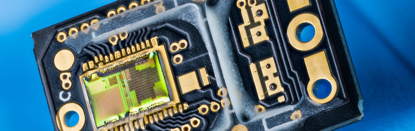
Research continues on improving printed frontside silver conductor line efficiency.
A simple Internet search will reveal the photovoltaic industry is working hard on higher aspect ratio frontside conductor grids as a route to greater solar cell efficiencies. This is because the conductors, typically screen-printed on a cell’s frontside, block sunlight from reaching the energy converting strata below, and the narrower they are, the less shadow they cast.
However, as it is essential they maintain their current carrying capacity, and as this is governed by their cross-sectional area, it follows that as their width decreases, their height must increase. Hence the need for a greater height/width ratio, or aspect ratio.
While the pursuit of higher aspect ratios is essential, this goes hand-in-hand with an equally important factor that until now has been largely overlooked: conductor uniformity. This will become a critical factor as feature miniaturization progresses, as a conductor with many high/wide and low/narrow points is less efficient than one that has the same cross-section throughout.
A team here has been conducting in-depth studies on this issue since 2008, with the aim of developing a method for improving the efficiency of printed frontside silver conductor lines. Recently, results of this ongoing work were presented at the 24th European Photovoltaic Solar Energy Conference in Hamburg.
As part of the study, the team looked at the relative merits and demerits of printing using conventional mesh printing screens versus two-layer electroformed nickel stencils, carrying out extensive tests on both to identify the features necessary for an optimized, high-aspect ratio printing process.
They also explored in detail a significant obstacle to achieving the improved levels of paste transfer efficiency required for higher aspect ratio conductors when printing with conventional mesh screens: The screen apertures are partly full of wire. The first problem is the volume of screen aperture occupied by the wire cannot be filled with paste; and, second, the wire presents a large surface area to which paste can stick instead of transferring to the wafer.
Indeed, when analyzing conductor structure, it was graphically clear that the intervals between the highs and lows in any conductor mirrored the intervals between the knuckles in the screen mesh.
Much has been done to mitigate this problem. Wire diameters have been reduced to a current industry standard of 20 to 25 µm, and this has greatly improved aspect ratio and conductor uniformity. However, there is a limit to how fine a wire can be used, especially considering a screen must be sufficiently robust to withstand 10,000 sweeps of a high-speed, high-pressure squeegee. There is also a cost issue: Fine, high mesh-count screens are more expensive than large diameter, low mesh-count screens.
One obvious solution is to remove the mesh from the apertures completely, and several successful attempts already have been made to do just that using two-layer electroformed stencils. Our team decided to explore this option using a number of high-precision, two-layer electroformed nickel stencils designed especially for the tests.
Two-layer stencils typically use a bottom nickel aperture layer in which the wafer pattern is formed. This is protected and stabilized by a top layer, which, in its coarsest form, is a simple perforated foil. Such stencils provide much improved paste transfer and conductor uniformity over mesh screens, but improvements can be achieved by replacing the standard perforated foil with one that has reinforced apertures similar to, and that correspond with, those in the bottom layer. Here, the challenge lies in precisely aligning the two layers, and in ensuring the apertures are well-engineered.
Using appropriate pastes and this more sophisticated approach to stencil design, improved aspect ratios were achieved, as line widths were decreased to 50 µm and conductor uniformity was significantly better than anything realized using mesh screens.
Given these results, the team noted two-layer metal stencils could potentially outperform the best emulsion mesh screens, but that several obstacles must be overcome before this technology can be implemented widely. First, whereas the photoimageable emulsion used for mesh screens is sufficiently elastic to provide a reliable gasket between the screen and the wafer’s textured surface, the bottom layer of a nickel stencil is unyielding and could cause silver paste to bleed, creating more problems than are solved. Also, the stencil’s bottom surface must be totally defect-free; nickel nodules could crack or even break the wafer as pressure is applied. Such stencils are also more expensive, and their use in high-definition work requires a high degree of technical skill.
Having said this, electroformed stencils do provide relatively open apertures. This, and the considerable advantages of mesh screens, led the team to develop a third option: a hybrid solution based on a conventional screen, but that replaces its wire mesh with a prefabricated electroformed nickel top layer with reinforced apertures similar to those used in two-layer electroformed stencils. This is coated on the underside with traditional photoimageable screen emulsion, enabling the team to maintain the ”soft contact” gasketing properties of screen emulsion while freeing the apertures considerably.
Details regarding a hybrid screen solution were presented at the Hamburg event. This hybrid technology is effectively a printing screen with almost no metal in the apertures that, once its design is optimized, should offer better paste transfer efficiency, aspect ratio and cross-sectional area uniformity than the alternatives from which it is derived. CA
Tom Falcon is senior process development specialist at DEK (dek.com); This email address is being protected from spambots. You need JavaScript enabled to view it..