Improved Electrolytic Copper Plating for Flex PWBs
A novel process is said to improve product interconnection and mechanical reliability.
Today, the most common flexible printed circuit substrates are 12.5 - 25 µm thick, with the trend toward even thinner materials. Two primary types of copper foil are used for flex: electrolytic copper foil and rolled copper foil. Electrolytic copper foils typically come in thicknesses of 18 or 12 µm, while most rolled copper foils are 18 µm thick. As with polyimide substrates, both types of copper foils are moving to thinner dimensions. Generally, rolled copper foils demonstrate flexural properties superior to those of electrolytic copper foil. Applications that require very high degrees of flexibility and reliability, such as HDD read-write heads, are dominated by rolled copper foils. However, in recent years, the flexural properties of electrolytic copper foil have been greatly improved and are gaining share in optical pickup applications.
Each of the three FPC categories – single-sided, double-sided, multilayer – requires somewhat different manufacturing processes. In addition, manufacturing processes for multilayer FPCs vary significantly, depending on the specifics of the desired circuit structure and performance characteristics.
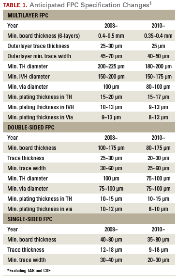
Table 1 demonstrates the evolution of FPC specifications. Design rules are changing to support miniaturization and multi-functionality. Trace widths and board thicknesses are becoming smaller. Minimum plating thicknesses are falling, leading to higher demands on the performance of plated copper deposits.
During double-sided/multilayer FPC manufacturing, metallization is employed to provide robust electric connections between layers. These processes represent critical steps within the overall production sequence. Typically, a combination of electroless copper plating and electrolytic copper plating is used to form plated through-holes and vias. Direct plate processes also are now widely used for initial metallization prior to electrolytic copper plating, especially for double-sided FPC.
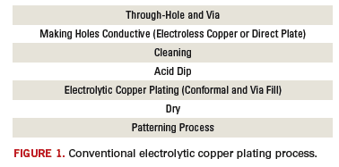
Electrolytic copper plating has a significant impact on FPC manufacture, as it affects wiring design, board dimensional tolerances and thermal/mechanical reliability. Figure 1 illustrates a conventional process flow for electrolytic copper plating. Electrolytic copper plating is carried out after the process steps of through-hole/via-hole formation, initial metallization process and pre-cleaning. Plated panels are dried prior to the patterning process. Since FPCs are thin and flexible, these features must be considered in their design and handling.
Electroplated copper deposits must have the following characteristics:
- Dimensional stability after plating (ensures stable wiring dimensions).
- Thermal/mechanical reliability (delivers appropriate performance for end-use environment and device assembly).
- Compatible with full range of making holes conductive chemistries.
- Uniform plating distribution on board surface (allows consistent circuit feature formation).
- Plating surface smoothness (eliminates surface defects that might reduce manufacturing yield or degrade flexural performance).
- Trends toward finer feature dimensions and higher interconnection densities require improved functionality from FPC electrolytic copper plating processes.
- The attributes and benefits of a new electrolytic copper plating process are illustrated by comparison with the performance of conventional processes.
Dimensional stability. In response to finer feature and higher interconnection density trends, registration tolerance has to be improved. Improved substrate dimensional stability during manufacturing is required to meet these targets for registration tolerance. The main factors affecting dimensional stability during FPC manufacturing are base material performance, plating deposit properties and manufacturing process conditions. Internal stress within electrolytic copper plating deposits plays an important part in determining the overall dimensional stability. The effect of plating stress manifests itself as either bowing of boards after etching or patterning, or as shifts in pattern feature locations. The board dimensions shrink when the deposit has tensile deposit stress and expands under compressive stress. FPCs are particularly influenced by internal stress because the boards are so thin and flexible.
Typically, the internal stress of acid copper deposits is tensile. The amount of internal stress changes gradually, due to structural changes associated with self-annealing of the deposit. A copper plating process having low internal stress is therefore preferred for FPC applications.
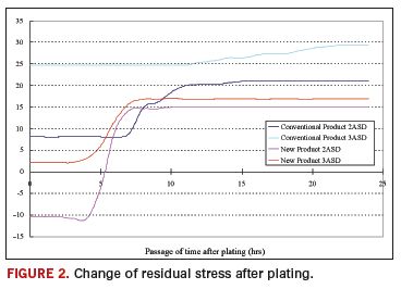
A spiral contractometer is most commonly used to measure stress in plated coatings. The deposit is formed on the exterior surface of a spiral shaped metal substrate, which is tightly secured at the lower end but free to move at the upper end. The interior surface is coated with an organic material to prevent deposition. Stresses within the deposit lead to either an opening or a tightening of the spriral, measured as an angular deflection of an indicator connected to the upper end. The deflection, combined with information on deposit thickness, then can be converted into a value for stress.
Figure 2 shows the residual stress for a conventional plating system and a newly developed bath, as a function of time after plating and plating current density. In a conventional process, deposit internal stress stabilizes between 20 - 30 MPa after 10 hr. While this level of residual stress is unlikely to have significant impacts on present FPC designs, it presents an issue for future design specifications. The new process shows an internal stress that reaches a value of approximately 15 MPa after 7 hr., and then remains stable. The residual stress is significantly lower than conventional processes.
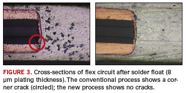
Thermal/mechanical reliability. Pb-free processing means higher assembly temperatures, placing greater demands on thermal reliability. The physical properties of electrolytic copper plating deposits must be enhanced to respond to these changes in assembly conditions and the trend toward finer feature dimensions. Figure 3 shows cross-sections of through-holes in FPCs after solder float testing and describes the substrate construction and test procedure. In general, when the plated deposits are thin (as is often the case in FPC applications), interconnection failures such as cracks tend to occur as a result of thermal shock. In tests, the new product shows excellent performance, even when used at low plating thicknesses. This provides an improved process window during assembly operations.
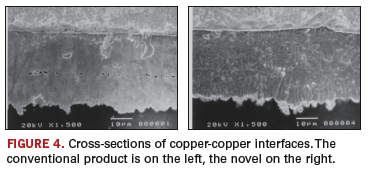
Compatibility with alternative metallization processes. Direct plating processes are widely used for the initial metallization of general-purpose, double-sided FPC. Compared to electroless copper plating, the resistance of the initial direct plate film is high, which poses a risk of deposition failure in the subsequent electrolytic copper plating process. In such cases, powdery copper deposits may be formed during the early stages of plating, resulting in adhesion defects and poor appearance. The new process has been found to show excellent compatibility with both a wide range of electroless copper and direct plate processes, providing excellent copper-to-copper interface quality (Figure 4).
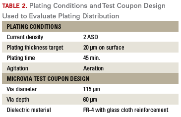
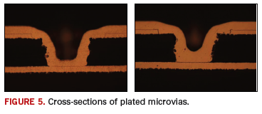
Plating distribution. Thinner copper foils and plated copper deposits and microvias are essential for increasing circuit density. High-density multilayer FPCs employ microvias for innerlayer connections. Consistent and uniform plating distribution is required to ensure optimum connection reliability, particularly for smaller diameter microvias (Table 2). Figure 5 compares coverage capabilities of electrolytic copper plating on microvias. The new process shows improved capability, even for small diameter vias, due to its plating coverage and distribution.
Surface smoothness. In contrast to rigid boards, FPCs require very high degrees of deposit flexibility. Bend test requirements for the FPC section that acts as an interconnection between boards vary widely with application. In the case of the interconnection within the hinge of a cell phone, more than 100,000 flexures are required (measured using a 180° open/close test).2
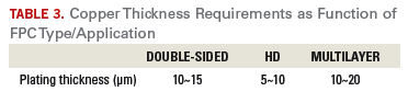
The area undergoing the bending operation must have a thin copper deposit in order to meet these needs. Table 3 shows examples of typical electrolytic copper plating thicknesses as a function of FPC type. FPCs used for moving parts generally use rolled copper foils, due to their superior bending performance. However, when electrolytic copper plating is applied over rolled copper foil, some degree of surface unevenness can sometimes be observed on the plated deposit. This is believed caused by an interaction between the plating process and the crystal structure of the foil substrate (Figure 6).
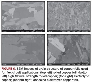
Ion polishing was used to prepare samples, which illustrate the differences in crystal structures between four different copper substrate materials (Table 4). 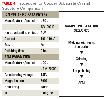
Unannealed electrolytic foils have relatively smaller grain sizes, while the grain sizes of rolled or annealed electroplated foils are larger (Figure 6).
Surface unevenness may lead to defects in subsequent imaging processes and can therefore become a major obstacle to high yield manufacture of finer line high-density FPC. To reduce the unevenness, higher plating thicknesses or mechanical polishing have been considered. However, thicker films have been observed to degrade flexural performance, and mechanical polishing is very difficult to perform, due to flex’s thin and soft properties. Electrolytic copper plating processes are required to produce deposits with excellent surface smoothness on all copper foils used for FPC to permit finer patterning and higher bending performance at reduced deposition thicknesses and without mechanical polishing.
When plating on rolled copper foils, conventional products often show some fine surface unevenness and a semi-bright appearance. In contrast, no surface unevenness is found with the novel product and good brightness is observed. The new process permits reduced plating thicknesses with excellent plated surface smoothness, which provides both fine patterning capability and improved flexural performance.
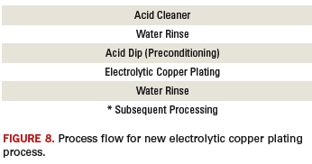
Figure 7 shows a comparison of deposit brightness between a conventional process and the new process. The latter does not require special process control, and conventional plating equipment may be used. Figure 8 shows the process flow of the new electrolytic copper plating. 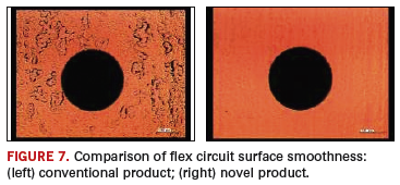
Ed.: Portions of this article were previously published.
References
1. Japan Jisso Technology Roadmap 2007, pp. 55-57, 63-65, 69-70.
2. M. Watanabe, H. Sakurai, and T. Kanagawa, ”The Future Trend and Characteristics of FPC,” Fujikura Gihou, vol. 109, pg. 33-34, 2005.
Hiroshi Hoshiyama is interconnect technology R&D director Japan; Shinjiroh Hayashi is interconnect technology R&D project leader; Makoto Sakai is interconnect technology R&D scientist, and Rikiya Shimizu is interconnect technology Japan/Korea marketing manager at Rohm and Haas Electronic Materials KK, a Dow Group Co. (rohmhaas.com).


