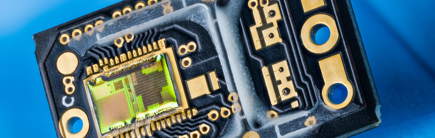
MicroBGAs provide electrical and physical advantages at the cost of increased design and manufacturing complexity.
The micro-ball grid array is one of the most advanced surface mount devices and is quickly becoming the package of choice for the electronic circuit designer. A microBGA is a subclass of the generic ball grid array (BGA). Typical BGA packages have ball-to-ball spacing of 1.0 mm or 0.8 mm, whereas typical microBGA packages have a pitch of about 0.4 mm or less. This permits package size reduction, among other advantages, plus microBGAs can be placed in close proximity on a printed circuit board (PCB).
Packaging technology plays a key role in device performance. In the past few years, innovative technologies have reduced chip delay in the actual IC semiconductor material. However, in a packaged IC, signal delay has not been able to be reduced as much. Thus, packages have become a bottleneck in high-speed systems. One of the best solutions is the micro BGA because it exhibits better chip delay performance when compared to other technologies.
Since the microBGA package is more compact than other SMT devices, it has a shorter contact length from the device pin to the outside world. Therefore, it provides a lower inductance/impedance path to all signals. It can keep pace with the advancement of IC semiconductor and logic implementation technologies and has minimized the signal losses by increasing the packaging density and reducing the packaging delay.
A microBGA’s electrical performance shows that it has low resistance, capacitance and inductance of the short beam leads. For high performance applications, an optional ground plane further reduces the self and mutual inductance, as well as cross talk.
While microBGAs represent a major innovation in component packaging, they pose a significant challenge for PCB design. A typical microBGA features 0.4-mm pitch, but the latest generation of fine pitch BGAs are as small as 0.3-mm and 0.25-mm pitch. PCB layout engineers must first find easier ways for pin fanout/routing solutions for 0.4-mm pitch BGAs, otherwise, routing complications can result. Consequently, those complications can cause an increase in layer count and sometimes call for high-end fabrication requirements.
This means that before finalizing a microBGA for design, the designer should carefully analyze the microBGA device’s details and make sure the balls’ pin pitch allows for all traces fanout/routing without using unnecessary special manufacturing requirements, and that it can be done within the allowed number of layers.
The designer’s intent is to optimize the number of layers required to route high pin count packages without affecting their performance. The pin assignment and pin grouping of the microBGAs can also be modified to enable efficient board routing with an optimum number of required board layers.
Chip manufacturers have detailed datasheets that include recommended land patterns. There are normally two types of land patterns used for BGA pads: Non soldermask-defined pads (NSMD) and soldermask-defined pads (SMD). FIGURE 1 illustrates the differences between the two land patterns.

NSMD pads have a soldermask opening that is larger than the pads, whereas SMD pads have a soldermask opening that is smaller than the copper pad. Most vendors suggest the use of NMSD because it provides tighter control of copper artwork registration compared to the positional tolerance of the soldermask process. This becomes more important when the PCB designer deals with fine pitch components like microBGAs.
The fanout/routing technique takes into account such factors as ball pitch, land diameter, number of I/O pins, via type, pad size, trace width/spacing and the number of layers required to escape the microBGA.
It’s not appropriate to have a traditional dog-bone fanout pattern for a microBGA because of its narrow pitch. This means either via-in-pad or blind/buried vias are used. The via- in-pad approach places a via directly under the device’s contact pads, filled with a conductive material, usually silver, which can provide a fairly flat surface This allows higher component density and improved routing.
FIGURE 2a shows the land pattern of a microBGA.

It’s obvious the traditional approach of BGA fan-out is not workable here. It means the designer has to use either via-in-pad or blind/buried vias or a combination of both. In order to make the design cost effective for fabrication, it is better to avoid blind/buried vias, but it really depends on the microBGA size and its pins assignment. As shown in FIGURE 2b, via-in-pads are used for internal pins, whereas outer pins are fanout with a regular via, away from the pins.

FIGURE 2c shows that the designer is able to fanout/route all microBGA pins with a regular 6 mil via size, in a minimum number of layers and without using any high-end fabrication technique. In this example, the microBGA has less pin count. For a greater number of pins, the designer either has to use blind/buried vias or via-in-pad with a high layer count stackup. This means that the PCB designer needs to do pre-calculations per the manufacturer’s recommended land pattern, gap between the pads, allowed number of layers and the minimum drill size that can be used in the design.

Decoupling the board’s power system has immense significance, especially for high-speed systems. The basic and most efficient way of utilizing decoupling capacitors is to place capacitors on the opposite side of the PCB with respect to the microBGA device and within the grid of vias and contacts used to route signal traces to the microBGA device.
Due to the small 0.4-mm pitch microBGA package size, it’s not possible to use 0201 or bigger capacitor packages directly underneath the device. Either a 01005 or smaller package (if available) can be used. This placement technique provides minimum inductance and maximum capacitance to decouple the IC’s power system. This placement is motivated by the practice of placing decoupling capacitors as close as possible to the power and ground pins of the subject device for optimum electrical decoupling performance. FIGURE 3a shows a 0.5 mm BGA with 0201 package size decoupling capacitors, while FIGURE 3b shows a 0.4-mm pitch BGA with 1005 package size decoupling capacitors.


However, this technique also has some disadvantages, such as increased constraints on the routing of signal traces within the microBGA grid, reduced reliability and increased cost. Other capacitor packages, including 0805, 0603, 0402 and 0201, can be used for decoupling the microBGA, but they should be placed as close as possible to power/ground pins in order get better results.
While designing the PCB, the designer should also keep in mind future problems that the board can face. During the component assembly process, the board can undergo different problems, especially if it contains fine pitch components like microBGAs. Many defects in microBGA packaging arise from an inappropriate re-flow profile. It is always recommended that while designing PCB layout, all the parts around the BGA should have a 20 mm to 25 mm clearance. This space facilitates the rework ability of the microBGA without damaging any other parts.
Use of microBGA packages increases the level of design complexity. Its narrow pitch creates a challenge for the PCB layout, as does the greater number of pins connecting to the design in a smaller area compared to a conventional BGA. Similarly, board fabrication may be required to undergo advanced techniques, resulting in cost increases. Fabrication facilities need to develop easier manufacturing solutions for such components and should be prepared for further finest pitch components.
A microBGA comes with considerable electrical and physical benefits. However, as with any technology, a microBGA is not without problems. For example, microBGA expertise is not commonly available, rework methods are more difficult, solder joint reliability is more critical, voiding becomes an increasingly critical issue and microBGA assembly inspection is more difficult.
Printing equipment needs to be properly calibrated, and quality paste needs be used in the assembly, especially for fine pitch components. These problems can be reduced or eliminated by optimizing the SMT process. Also, a properly designed PCB layout includes considerations for all fabrication and assembly problems. This approach considerably helps to successfully finalize a microBGA project and achieve higher yield. PCD&F
Ishtiaq Safdar is a PCB layout engineer with NexLogic Technologies, San Jose, CA; This email address is being protected from spambots. You need JavaScript enabled to view it..